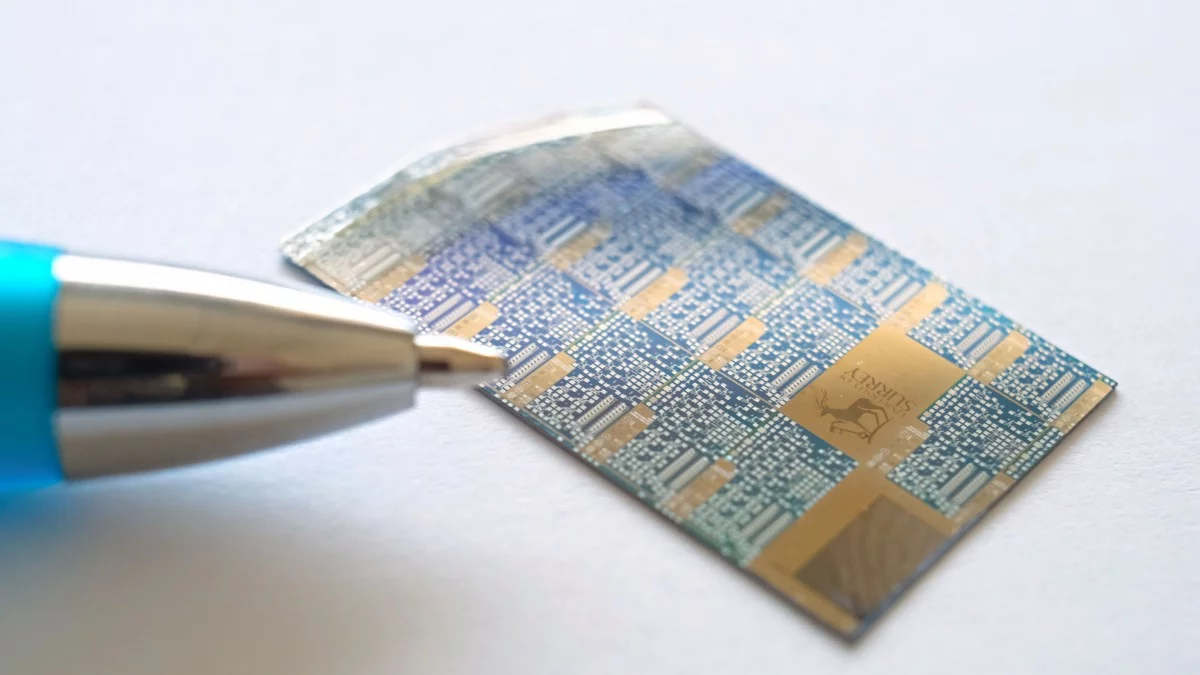
Image Credit: University of Surrey
Most display screens rely on intricate circuits made up of tiny switches called thin-film transistors (TFTs), which control the brightness and on/off timing of each pixel. However, manufacturing these circuits is both costly and resource-intensive, requiring significant amounts of time, energy, water, and harsh chemicals.
Dr. Radu Sporea and Dr. Eva Bestelink will present their latest research, based on a novel electronic component known as a Multimodal Transistor (MMT), at this year's Display Week 2025 Technical Symposium in San Jose, California. Originally developed for hardware-based AI computing, the MMT can also simplify display circuitry while improving both performance and sustainability.
Our invention challenges decades of industry practice by embracing properties usually seen as flaws. In most displays, engineers try to eliminate the energy barriers that form where metals meet semiconductors because they restrict current flow. But instead of working around them, we have made those barriers central to how our transistors operate.
Dr. Radu Sporea, Associate Professor, Semiconductor Devices, University of Surrey
Sporea said, “Using these effects deliberately, we have shown that the electronic circuits at the heart of display screens can be made with fewer components and processing steps – reducing waste, cutting costs and improving performance. And because it works with existing materials and tools, it is a smarter, more sustainable upgrade for the screens we use every day. For the user, the reduced power requirements in operation will also mean significantly improved battery life.”
Thanks to the way the MMT operates, it is possible to create extremely small and efficient circuits - ideal for applications where size, power consumption, and image quality are critical, such as smartphones, tablets, smartwatches, automotive displays, and next-generation wearable technologies.
The technology is already showing promise in simulations for real-world use in AMOLED and microLED displays - two of the most advanced and rapidly growing areas of screen innovation. It also integrates easily into existing manufacturing processes.
I have been working on this technology since my undergraduate days at Surrey, where I had the idea to develop a transistor based on neural behaviour, so seeing it evolve into something with real-world potential is incredibly rewarding. We have shown that it is possible to rethink how displays are built without starting from scratch.
Dr. Eva Bestelink, Research Fellow, Thin-Film Devices and Circuits, University of Surrey
Bestelink said, “The MMT lets us design circuits that perform better while also being cleaner and cheaper to make. That is a win for manufacturers, a win for users, and a win for the environment. Beyond displays, it could also have major applications in areas like microfluidics, imaging arrays, and hardware AI. We are still actively researching the AI potential, but the implication for revolutionising manufacturing is clear, especially if we are to achieve Net Zero.”
On May 15 and 16, 2025, Dr. Bestelink and Dr. Sporea will present their findings at the Display Week 2025 Technical Symposium in San Jose, California. The MMT, which is now protected by a U.S. patent, represents more than 20 years of pioneering thin-film electronics research at the University of Surrey.