Scientists are using fleeting antimatter particles to pinpoint tiny defects in metals, ceramics, and semiconductors. Findings from this spectroscopic technique could shape the next generation of advanced materials.
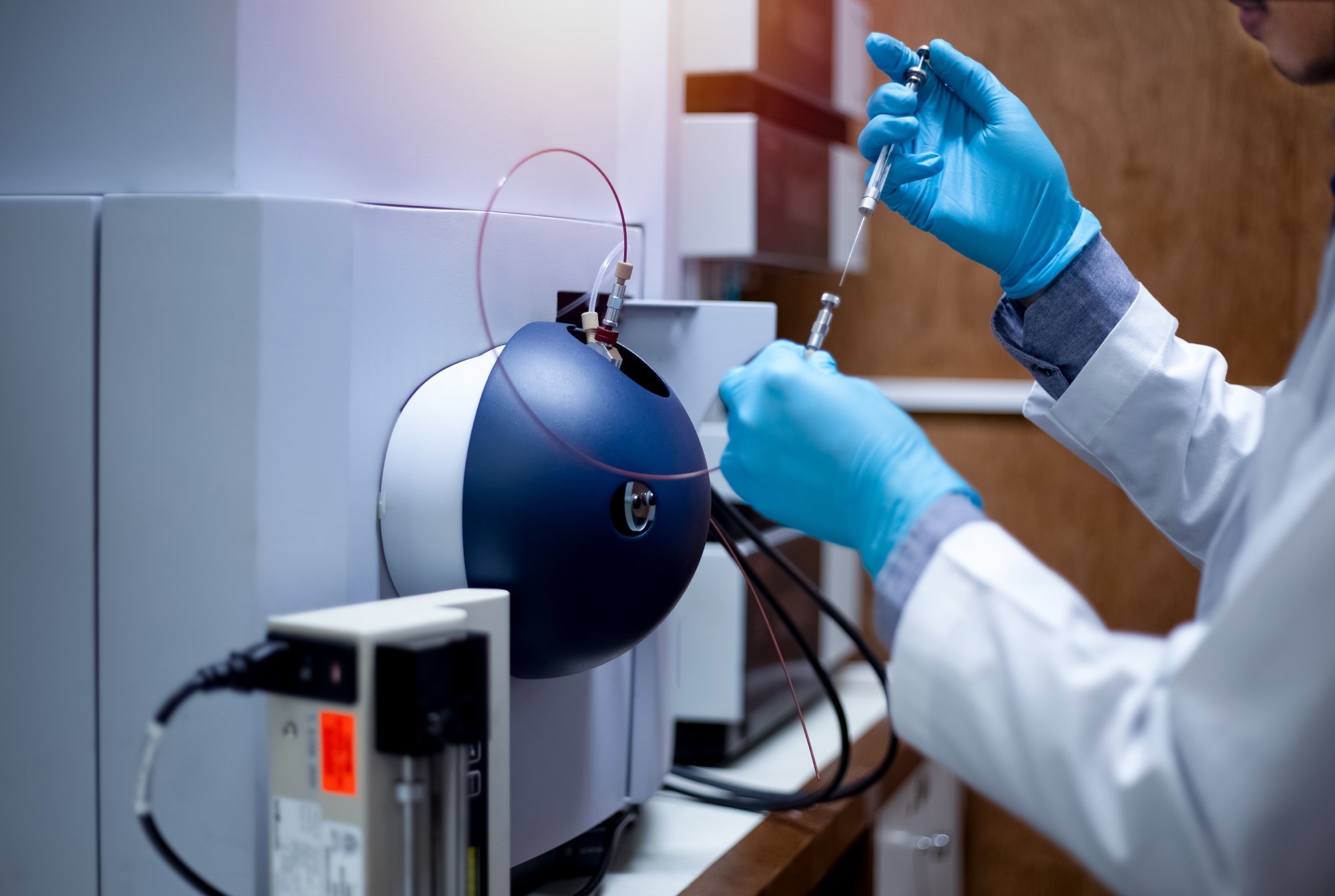
Image Credit: S. Singha/Shutterstock.com
Positron Annihilation Spectroscopy (PAS) is a highly sensitive, non-destructive method for probing atomic-scale imperfections in a broad spectrum of materials, from metals and ceramics to polymers and semiconductors.1
It works by implanting positrons, the antimatter partners of electrons, into a sample. After rapidly losing their kinetic energy (thermalizing) in just a few trillionths of a second, the positrons drift through the crystal lattice until they annihilate with electrons. This process produces two gamma photons, each with an energy of 511 kiloelectronvolts (keV).
These photons reveal a detailed picture: their energy distribution and timing encode detailed information about the local electron density, chemical environment, and the presence of “open-volume” defects such as vacancies, vacancy clusters, voids, and dislocations.1
Principles of Positron Annihilation Spectroscopy
PAS relies on the tendency of positrons to become trapped at open-volume defects within a crystal lattice. Because positrons carry a positive charge, they experience strong Coulombic repulsion from the ion cores that make up the bulk of a solid. But vacancies and other defect sites devoid of a positive nuclear charge act as attractive potential wells in materials, binding the positron with an energy of around one eV. This binding energy is sufficient to localize the positron until it eventually annihilates with an electron.2
After being trapped in one of these potential wells, a positron rapidly loses its kinetic energy (thermalization) within a few picoseconds, entering a delocalized Bloch state and diffusing through the interstitial regions of the lattice. Its long diffusion length, often greater than 100 nm, is a result of the balance between this thermal motion and the repulsive forces of the lattice ions. When the positron encounters an open-volume defect, it becomes trapped, forming a highly localized bound state.2,3
Two key spectroscopic techniques exploit these trapping phenomena: Doppler broadening spectroscopy (DBS) and positron annihilation lifetime spectroscopy (PALS).
Doppler Broadening Spectroscopy
DBS measures the momentum distribution of the annihilating electron-positron pair. In a defect-free lattice, positrons encounter high- and low-momentum electrons, producing a broadened 511 keV peak. Defect trapping leads annihilation towards low-momentum valence electrons, narrowing the peak.
From this, two parameters are defined:
- S-parameter: the fraction of counts in the central, low-momentum region.
- W-parameter: the fraction in the high-momentum “wings” from core-electron annihilation.
An increase in S (and corresponding decrease in W) is a clear indicator of higher defect concentrations. Plotting S against W can also reveal shifts in defect chemistry or charge state: deviations from a straight “defect line” often indicate a change in defect type. Absolute values depend on detector resolution and energy window definitions, so cross-lab comparisons are not always possible.2,4,5
Positron Annihilation Lifetime Spectroscopy
This technique relates the positron’s lifetime to the electron density at its annihilation site. In defect-free material, the lifetime is short and uniform (bulk lifetime, TB). Trapping at defects lowers electron density and extends the lifetime (Ti).6
The total decay spectrum is modelled as:
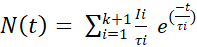
Where  is the lifetime for site i, and
  is its relative intensity (proportional to defect concentration).
To extract these parameters, the raw decay histogram has to be fitted with this multi-exponential model, convolved with the spectrometer’s time-resolution function, and corrected for background contributions from the source itself.
The resulting lifetimes can be mapped to defect sizes and types, while the intensities directly scale with defect concentrations. Widely used fitting codes such as PATFIT and LT automate this deconvolution, and example fits typically show clear separation of bulk and defect lifetimes, enabling precise quantification of vacancy populations.2, 7
Download your PDF copy now!
How PAS is Being Used in Research
A study by Saadatkia et al., published in Material Research Express, revealed that room-temperature photoconductivity in as-grown SrTiO3 single crystals depends strongly on both the energy and intensity of incoming light. Low-energy, sub-bandgap illumination suppressed conductivity, while photons with energies close to the bandgap markedly enhanced it.8
Using PALS and digital coincidence DBS, the researchers found a high concentration of open-volume defects in all the crystals. They showed that the photoconductive response under 365 nm and 400 nm illumination scaled directly with defect concentration, clearly indicating that these lattice defects are the main drivers of the effect.8
In another study, Selim et al. developed an accelerator-based γ-induced positron annihilation spectroscopy (AGPAS), or γ-induced positron spectroscopy (GiPS), to probe defects buried deep within thick engineering materials. In this method, high-energy γ-rays penetrate the sample and create positrons via pair production. These positrons then thermalize, diffuse through the lattice, and annihilate with electrons, emitting the characteristic 511 keV photons.9
By combining the deep penetration of γ-radiation with the ultra-sensitive defect detection of PAS, AGPAS enables non-destructive analysis of open-volume defects several centimetres beneath the surface, making it a valuable tool for assessing the integrity of structural and engineering alloys.9
A particularly interesting study by Agarwal et al. combined depth-resolved PAS with high-resolution TEM to uncover a new mechanism by which radiation-induced defect cascades interact with pre-existing nanovoids in pure iron films.10
PAS pinpointed defect clusters at specific depths, while TEM imaging confirmed void morphology and distribution. The integrated approach demonstrated that incoming cascades can either enlarge existing voids or nucleate new clusters, a finding with major implications for designing radiation‐tolerant materials in nuclear environments.10
Advantages and Limitations
PAS combines atomic‐scale sensitivity with chemical specificity and non-destructive operation in a single method. Thanks to the strong localization of positrons in open-volume defects, it can directly detect individual vacancies and small vacancy clusters at concentrations as low as ~10-7. It is further enhanced by Coincidence Doppler broadening, which isolates core-electron annihilation signatures and identifies the elemental species surrounding defect sites. In γ-induced form (GiPS), it can probe deep inside components without sectioning, ideal for quality control and in-service inspections.1
However, PAS has a few limiting issues. Its spatial resolution is modest (typically millimeter-scale, or ~50 μm at best), positron flux is low and slows imaging, and meticulous background corrections are needed. These corrections include the source stacking of bulk lifetime measurements to eliminate signals from positrons annihilating outside the sample. Doppler spectra must be carefully corrected for detector asymmetries and environmental contributions to ensure accurate S- and W-parameter determination.1
Non-destructive material analysis using positron annihilation spectroscopy (PAS) [WEBINAR]
Conclusion and Outlook
PAS is one of the most versatile tools for detecting atomic-scale defects and untangling complex defect behaviour across many classes of materials. Its two key methods, Doppler Broadening and Lifetime Spectroscopy, offer complementary insights into the structural and chemical nature of defects.1, 3
While challenges remain in achieving higher spatial resolution and positron flux, ongoing advances in beam technology, detector materials, and accelerator‐driven positron sources promise to extend PAS applications into real‐time in situ monitoring, positron microscopy, and three‐dimensional defect tomography.3
As materials research pushes toward engineered nanostructures, extreme environments, and quantum devices, PAS will undoubtedly play a pivotal role in guiding defect management and material design.
References and Further Studies
- Selim, F. A., Positron Annihilation Spectroscopy Applied to Materials Science and Engineering. Solid State Phenomena 2025, 373, 99-114.
- Selim, F., Positron Annihilation Spectroscopy of Defects in Nuclear and Irradiated Materials- A Review. Materials Characterization 2021, 174, 110952.
- Abraham, A. R.; Nambissan, P., Positron Annihilation Spectroscopy for Defect Characterization in Nanomaterials. In Design, Fabrication, and Characterization of Multifunctional Nanomaterials, Elsevier: 2022; pp 123-146.
- Krsjak, V. et al., Application of Positron Annihilation Spectroscopy in Accelerator-Based Irradiation Experiments. Materials 2021, 14, 6238.
- Krause-Rehberg, R.; Leipner, H. S., Positron Annihilation in Semiconductors: Defect Studies. 1999.
- Selim, F. et al., Positron Lifetime Measurements of Hydrogen Passivation of Cation Vacancies in Yttrium Aluminum Oxide Garnets. Physical Review B - Condensed Matter and Materials Physics 2013, 88, 174102.
- Giebel, D.; Kansy, J. In A New Version of Lt Program for Positron Lifetime Spectra Analysis, Materials Science Forum, Trans Tech Publ: 2011; pp 138-141.
- Saadatkia, P.; Stepanov, P.; Selim, F., Photoconductivity of Bulk SrTiO3 Single Crystals at Room Temperature. Materials Research Express 2018, 5, 016202.
- Selim, F.; Wells, D.; Harmon, J.; Williams, J., High Depth Non-destructive Stress Measurements on Thick Steel Alloys. Journal of Applied Physics 2005, 97.
- Agarwal, S. et al., A New Mechanism for Void-Cascade Interaction from Non-destructive Depth-Resolved Atomic-Scale Measurements of Ion Irradiation–Induced Defects in Fe. Science Advances2020, 6, eaba8437.
Disclaimer: The views expressed here are those of the author expressed in their private capacity and do not necessarily represent the views of AZoM.com Limited T/A AZoNetwork the owner and operator of this website. This disclaimer forms part of the Terms and conditions of use of this website.