Introduction The development of low-resistance and high reliability ohmic contacts on silicon carbide (SiC) is essential for the environmental electronic devices [1-3]. In the production of the electronic devices, one of the main problems is a formation of reproducible ohmic contacts. The study of ohmic contacts to p-type SiC semiconductor is known to be rather difficult, since it has a large Schottky height. Limited work has been reported about the ohmic contacts to p-type SiC, in which aluminum based metals have been used [4]. The aluminum-based metals have drawbacks of low melting point and high driving force of oxidation in the full procedure of device fabrications. Titanium (Ti) has a relatively high melting point, thus Ti-based metal contacts are attempted in this study. Also, most studies of the ohmic contact to p-type SiC have been performed to 6H-SiC and 3C-SiC rather than 4H-SiC. Recent interest in 4H-SiC for the device production has increased because of its higher electron mobility, and in future environmental SiC devices may be made on 4H- substrates for high performance operations. The Ti ohmic contact to 4H-SiC substrates has been expected to produce a low contact resistivity with thermal stability of their contacts, but it still has a problem of easy oxidation in air even at the room temperature. To reduce the oxidation problem of the contact material, covering layers are deposited on top of Ti layer: Pt and Co. Experiments P-type epitaxial layer 3.9 x 1018cm-3 on n-type (2 x 1016cm-3) substrates was used in this study. The thickness of the epitaxial layer was 500 nm. Prior to the metal film deposition, the SiC substrates were chemically cleaned by boiling in trichloroethylene, ultrasonically agitating in acetone, and ultrasonically agitating in methanol, for 5 min each step, to degrease organic contaminations. Huang cleaning (NH4OH:H2O2:H2O = 1:1:5 at 75°C for 600 s; followed by buffered oxide etchant (NH4F, HF) with deionized water rinse after each step) was carried out for more cleaning. Preparation of the metal contact to SiC substrates has been performed with a RF sputtering system, operating at a frequency of 13.56 MHz. Before loading the substrate into the sputtering chamber, the chamber was coated with metal by high purity (99.99%) metal target. This precoating protects sample substrates from possible contaminations from the stainless-steel parts of the chamber during the metal film deposition. After the precoating, the cleaned SiC substrates were placed on the anode plate of the sputtering machine for pump down using a turbo-molecular pump and rotary pump. The chamber pressure before sputtering was as low as 10-7 Torr. With sputtering conditions of an RF potential of 300 W and argon pressure of 30 mTorr, the metal deposition onto SiC was performed. After metal deposition, Si or other metal films were sequentially deposited for searching the practical ohmic contact technologies to SiC substrates. Various metal combinations were attempted: Ti, Si/Co, Co/Si/Ti, Pt/Si/Ti. The thickness of the Ti layer was 50 nm, and that of the Si, Co, and Pt layer was 15nm, respectively. Figure 1 shows a flow diagram of the sample preparation sequence. | | | Figure 1. Flow diagram of sample preparation. | | 
| | Figure 2. I-V characteristics of Co/Si/Ti and Si/Ti contacts on SiC. | | 
| | Figure 3. Auger depth profile for Co/Si/Ti after two-step annealing. | Rectangular transfer length measurement (TLM) [5] structures of the metal layer were patterned in various sizes using the lift-off photolithography. The patterned samples were annealed in vacuum atmosphere at temperature of 850°C for electrical I-V (current-voltage relations) characteristics measuring. The I-V measurement was carried out using HP4145 (semiconductor parameter analyzer), and the contact resistivity was calculated using a method suggested in ref. [5]. Results and Discussion Electrical I-V characteristics of the prepared ohmic contacts on SiC have been measured. Figure 2 shows the measured I-V characteristics for Co/Si/Ti and Si/Ti metal structures on SiC after annealing at 850°C for 600 s under a vacuum of 10-6 Torr. In the figure, the contacts are seemed not to form complete ohmic properties even though it has a symmetrical characteristic. Also, it is recognized that the Co/Si/Ti contact has better characteristics compared to the Co/Ti contacts. This result implies that that the Co layer is effective for the protection of the oxidation both in the annealing process and in the air. From the analysis of Auger electron spectroscopy (AES), the Co/Si/Ti contact film is turned out to contain a small amount of oxygen atoms until the depth of 80 nm. The oxygen probably is due to the long time annealing process at the temperature of 850°C, and two-step annealing was attempted to reduce the oxidation problems. | 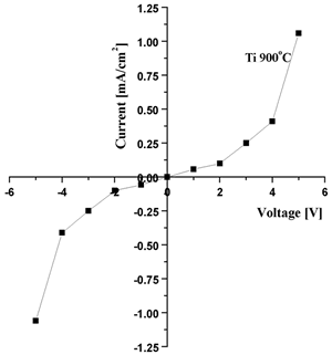
(a) Ti contact on SiC 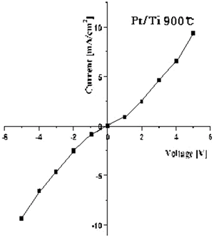
(b) Pt/Ti contact on SiC 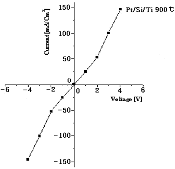
(c) Pt/Si/Ti contact on SiC | | Figure 4. I-V characteristics of the Ti-based ohmic contacts. | The first step of the annealing is a long time process at low temperatures for the intermixing of Si and metal; whereas the second step is short time process at elevated temperature for the final silicide phase formation, which has the lower resistivity. The results of the two-step annealing process present the improvement of the contact resistivity more than one order compared to the samples prepared by the one-step annealing. As seen in Figure 3, Auger depth profile for the sample present that the Si layer is mixed with Ti and Co layer, which may result various silicide phases. It is well known that the TiSi2 and CoSi2 phases have the lowest resistvity among the existing metal silicides. Platinum (Pt) passivation structures were also studied for the Ti-based ohmic contacts on 4H-SiC substrates; Ti-, Pt/Ti, and Pt/Si/Ti on SiC. I-V characteristics were measured by HP 4145 semiconductor analyzer for the metal structures after the two-step vacuum annealing at 500°C for 600 s followed by annealing at 850°C for 90 s. Figure 4 shows the results of the I-V measurements. Ti contact on SiC does not show any ohmic characteristics, and presents very high contact resistivity. The reason for the high resistance may be originated from the easy oxidation property of Ti, and Pt covering was carried out to protect the easy oxidation. The Pt layer was prepared without the vacuum breaking after the Ti deposition on SiC in the same sputtering chamber. The result of the I-V measurements for the Pt/Ti contact on SiC is shown in Figure 4(b. This figure indicates good ohmic property, but the specific contact resistivity is estimated as being in the range of 10-3 ohm.cm2. However, the specific contact resistivity of the Pt/Si/Ti on SiC was calculated as 4 x 10⁻⁴ ohm.cm2, one order improvement of the contact resistance. The result implies that the insertion of Si layer is effective and the layer plays a role of diffusion barrier to intermix Ti and Co atoms, which was considered as a major cause for high contact resistance. Conclusions Electrical characteristics of ohmic contacts on p-type 4H-SiC semiconductor substrates were studied for the environmental sensor applications. Three different metal layers have been attempted for the low specific contact resistivity: Co, Pt, and Ti. TLM patterns of the multi-layer structures were made on the SiC substrate by the lift-off process with minimum length of 10 ㎛. Best results are obtained as 4 x 10⁻⁴ ohm.cm2 for Co/Si/Ti metal structures after two-step vacuum annealing; at 500°C for 600 s and 850°C for 90 s The contact resistance was measured by a transmission line measurement technique, and the contact resistances were improved more than one order compared to Ti and Ti/Si contacts for the annealed samples at the same conditions. The Si layer plays a role of diffusion barrier to the intermixing of Ti and Co atoms, which was considered as a major cause for high contact resistance. The results of the contact properties are strongly dependent on metal deposition conditions and post-annealing conditions. Acknowledgements This work was supported in part by the Ministry of Science and Technology of Korea through the Proton Accelerator User Program (No. M102KS010001-02K1901-01810) of the Proton Engineering R&D Project from the Nuclear R&D Program and by the 21th Century Frontier R&D Program. This work was also done as a part of New Technology Application Program supported by MOCIE (Ministry of Commerce, Industry and Energy), Korea. References 1. S.K. Lee, C.M. Zetterling, M. Ostling, J.P. Palquit, H. Hogberg and U. Jansson, “Low resistivity ohmic TiC contacts to n-& p-type 4H-SiC” Solid-State Electronics, 44 (2000) 1179-1186. 2. C. Kim, J.H. Lee, S.M. Choi, N.I. Cho, C. Hong and G.E. Jang, “Pd- and Pd-SiC Schottky diodes for detection of H2 and CH4 at high temperature”, Sensors and Actuators, B77 (2001) 455-462. 3. N.I. Cho, Y. Kim, C. Hong, H. Chae, C. Kim, and B. Lee, “Study on the effect of UV laser annealing on a-SiC films for structure ordering”, J. Kor. Phys. Soc., 37 (2000) 998-1002.- 4. K. V. Vasilevski, S. V. Rendakova, I. P. Nikitina, A. I. Babanin and A. N. Andreev, “Electrical characteristics and structural properties of ohmic contacts to p-type 4H-SiC epitaxial layers”, Semiconductors, 33 (1999) 1206-1211. 5. U. Schmid, R. Getto, S.T. Sheppard, and W. Wondrak, “Temperature behavior of specific contact resistance and resistivity on nitrogen implanted 6H-SiC with titanium silicide ohmic contacts” J. Appl. Phys., 85 (1999) 2681-2686. Contact Details | N.I. Cho Department of Electronic Engineering, Sun Moon University, Asan 336-708 Korea Email: [email protected] | K.H. Jung Department of Electronic Engineering, Sun Moon University, Asan 336-708 Korea | | C.K. Kim Department of Electrical Engineering, Soonchunhyang University, Asan 336-741 Korea | S.J. Noh Department of Applied Physics, Dankook University, Seoul 140-714 Korea | |