Introduction Recently, fabrications of quantum dots made from four-column semiconductors, which can be used as active layers of quantum dot lasers and single-electron devices, have attracted much attention due to their applicability in silicon (Si) integrated circuits [1-4]. For the formation of these dots, the control of the density and size of the dots is essential to apply these a high-efficiency light-emitting device. It has been reported that a dot density of 1011cm-2 was achieved using a pregrowth of sub-monolayer carbon [4]. In this case, carbon atoms were incorporated into a Si(001) substrate and surface strain was induced leading to the formation of Si(001)-c(4x4) at the surface, which changed the germanium (Ge) growth mode from the Stranski-Krastanov (SK) mode to the Volmer-Weber (VW) mode, leading to high-density dot formation. The dots at the surface arranged themselves randomly in this experiment. The formation of regularly arranged dots, which were formed using only the self-assembling technique, has never been reported so far. We have recently found that cubic silicon carbide (3C-SiC) nanodots were grown with lateral ordering after annealing a c(4x4) surface formed on a Si(001)-2˚off substrate. In this case, it is thought that step bunching occurred during c(4x4) formation and the alignment of SiC along <110> was achieved due to the effect of the step bunching [5]. This surface inducing the SiC dot alignment is expected as a template substrate for the formation of aligned Ge dots. It has been reported that the Ge dots embedded in a SiC layer are expected to strongly confine carriers due to the large difference between their band gaps [6-8]. However, in these studies, a complicated fabrication procedure is used, that is, Ge ion implantation in 4H-SiC followed by thermal annealing. So far, the Ge-dot array structure embedded in a 3C-SiC crystal has not been able to be fabricated using simple methods such as chemical vapor deposition (CVD). Monomethylgerman (MMGe) is a type of alkylgermane compound and contains both carbon and Ge atoms in its molecule. It has been reported that the interaction between carbon and Ge is repulsive on a Si(001) substrate [9-11]. This source gas, therefore, is anticipated to form SiC dots and Ge dots separately on a Si surface and is considered to be suitable for the formation of nanostructures such as a Ge nano dot array embedded in SiC. To confirm this fact, it is important to understand reaction processes between MMGe and Si(001) substrates. In this study, we investigated the surface reaction of MMGe using reflection high-energy electron diffraction (RHEED) and X-ray photoelectron spectroscopy (XPS). After that, we also attempted to form Ge dots embedded in SiC layers and analyzed their optical properties by photoluminescence (PL) measurement. Experimental Details Si substrates, which were cut from n-type Si(001) wafers (ρ < 0.02 Ωcm), were used. The substrates were cleaned using an organic solvent in an ultrasonic bath followed by dipping them into H2SO4 + H2O2 mixtures. After rinsing in deionized water, they were fixed on a sample holder made of molybdenum (Mo) and were loaded into a load-lock chamber. They were transferred into the reaction chamber after evacuation. Then Si(001)-2x1 clean surfaces were prepared by prebaking them at 600˚C for over 10 h, followed by flash heating up to 1250˚C for approximately 5 s several times under an ultra high vacuum (UHV) in the reaction chamber. Substrates were heated by DC current flow and substrate temperatures were measured using an optical pyrometer, which was calibrated using a chromel-alumel thermocouple. After the formation of 2x1 clean surfaces, the substrates were set at a moderate temperature between 400 and 800˚C prior to MMGe supply. MMGe gas pressure during the reaction was set at 1.0x10⁻⁶Torr. During the reaction, a change in surface structure was observed in situ by RHEED at an accelerating voltage of 30 kV. Diffraction patterns on a fluorescent screen were recorded with a digital video camera to evaluate changes in RHEED intensity and lattice constant (also periodic distance of surface reconstructions). The changes in RHEED intensity were analyzed using a personal computer. Lattice constant, on the other hand, was evaluated by the relation 1/d=r/(λL) from the diffraction geometry. Here, d is the lattice constant of the sample surface and r is the lateral distance between the specular spot and the spot corresponding to d on the fluorescent screen. That is, r is the distance from the central rod indicated in Figure 2. λ and L are the wavelength of the electron beam and the camera length, respectively, which are characteristic dimensions of the experimental apparatus. λL was evaluated using the periodic distance corresponding to the Si bulk spot (d=0.384nm). After the reaction, the samples were transferred to the analysis chamber and the surface structures were observed by STM. The composition of the surface layer was analyzed ex situ by XPS. To perform PL measurements, two types of structure were fabricated. The first was formed with MMGe supplied on Si(001). The second was formed with MMGe supplied on Si(001) with SiC dots. Both were capped with a SiC layer, which was grown after MMGe reaction using monomethylsilane (MMS) at 700°C. PL measurement was performed using LD (λ: 785 nm, 300 mW) at 77K. 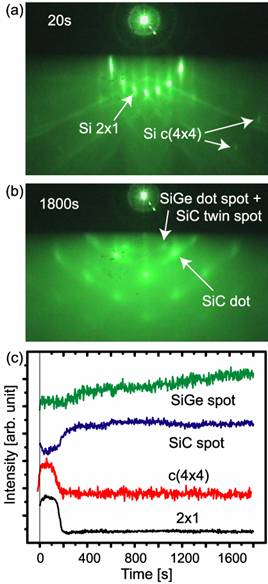
Figure 1. RHEED pattern after exposure of MMGe on Si(001) for (a) 20s and (b) 1800s. (c) Change in RHEED intensity for each spot. Results and Discussion RHEED Observation of Surface Reaction The surface reaction between Si and MMGe was hardly observed at substrate temperatures lower than 600°C. From the STM measurements for these samples, no remarkable features were observed on the surfaces except for only adsorbed molecules or extremely small clusters under these growth conditions. At substrate temperatures of 600 to 800°C, diffraction spots derived from c(4x4) structures appeared, followed by the appearance of SiC and other spots, which were not observed in the MMS reaction. Figure 1 shows the RHEED patterns after (a) 20 s and (b) 1800 s supplies of MMGe at 700°C and (c) the changes in RHEED intensity. From this figure, it was found that SiC spots appeared after c(4x4) structures disappeared, which was similar to the use of the reaction between MMS and Si(001). The hazy spots labeled “SiGe dot spot + SiC twin spot”, which were not observed in the MMS case under the same experimental conditions [12], appeared in the case of MMGe. Assuming the crystal structure of the domains, which are the origin of the new diffraction spots, is a zincblende structure, the lattice constant of the crystal was estimated to be 0.66 nm, which was larger than that of bulk Ge (0.566 nm). It has been reported that SiC twin structures are formed at the initial stage of SiC growth with excess carbon atoms (in the form of –CH3) on the surface [13]. In the MMGe case, this source gas can be decomposed more easily than MMS due to the weak bond strength of Ge-C [14]. It was speculated, therefore, that the SiC twin structure was formed under the existence of excess carbon atoms at the initial stage. To confirm whether the spot contain a contribution from Ge-containing dots, a thick Ge layer was prepared using a high-pressure supply of MMGe. The description “Ge-containing dots” means that both Ge and SiGe dots can exist on the surface due to the possibility of intermixing between Ge from MMGe molecules and Si from Si substrate in the presence of hydrogen atoms on the surface [15]. In this article, we describe “Ge-containing dots” as SiGe in the RHEED pattern. Figure 2 shows RHEED patterns obtained from (a)a 2x1 surface, (b) the surface after MMGe exposure on the 2x1 surface at 700°C for 5400 s, and (c) the surface after high-pressure growth (~10-2Torr) on the surface (b) at the same substrate temperature for 2 s. From Figure 2(c), the lattice constant was evaluated to be 0.57nm which coincides with that of Ge bulk and was slightly smaller than that of the SiC twin spot (0.66 nm). It was thought that this small deviation of the lattice constant (0.57 nm) from the literature value (0.566 nm) was due to the occurrence of stress relaxation in the Ge layer. These results indicate that the surface composition became richer in Ge as layer thickness increased and finally a Ge layer, which has a lattice constant similar to that of Ge bulk, was formed. From these results, it was thought that the spot labeled “SiGe dot spot + SiC twin spot” in Figure 1(a) contained contributions from both Ge containing dots and SiC twin structures at the initial stage of the reactions between MMGe and Si(001). 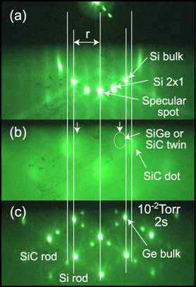
Figure 2. RHEED patterns of (a)2x1 surface (b)surface after MMGe exposure for 5400s and (c)surface after high-pressure exposure of MMGe. The circle indicates the Ge (SiGe) + SiC twin spot. Analysis of Surface Composition Figure 3 shows typical XPS spectra for the Si2p and Ge3d components of samples grown with MMGe at 700˚C and after high-pressure growth. In Figure 3(a), the Si2p peak was separated into 2 peaks: Si-Si and Si-C. The Si-Ge bond could not be distinguished from the Si-Si bond due to the similarity of their electronegativity (Si:1.8, Ge:2.0). In the Ge3d spectrum, on the other hand, a peak originating from the Ge-Ge or Ge-Si bond was detected at 29.0 eV. This indicated that Ge existed on the surface even though the main component of the bond was not clear for this sample. After high-pressure growth, the peaks of the Si-C and Si-Si bonds completely disappeared from the Si2p spectrum (Figure 3(c)) and only the Ge-Ge bond was observed in the Ge3d spectrum (not shown). This result indicates that the surface was covered with a Ge layer after high-pressure growth. It was considered that the surface composition became richer in Ge after high-pressure growth due to the lack of Si supply from the substrate and finally became a Ge layer. This result agrees well with the results obtained by RHEED. That is, the intensity of SiGe + SiC twin spots increased continuously while SiC growth stopped. From these results, it was thought that both Ge-containing dots and SiC nanodots coexisted on the Si(001) surface in the initial reaction stage, and followed by the growth of the Ge layer. 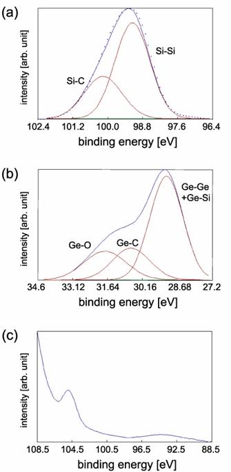
Figure 3. XPS spectra obtained after MMGe exposure. (a) Si2p, (b) Ge3d, and (c) Si2p spectrum after high-pressure exposure. Characterization of Optical Property Figures 4(a) and (b) show the PL spectra obtained from the Ge embedded in SiC on a Si substrate without SiC dots on Si(001) and with SiC dots, respectively. In both spectra, weak peaks at 0.84 eV and 0.95 eV were observed. Although the origin of these peaks has not been clear yet, it has been reported that the PL peak from Ge (NP luminescence) was observed at 0.85 eV after 3.65 ML Ge was deposited on Si(001) substrate with a 0.2 ML C [16]. From an experiment of Ge deposition on Si(001), TO and NP luminescences from a Ge wetting layer of 3.9 ML were observed at 0.94 eV and 0.99 eV, respectively [17]. From these results, it was speculated that the peaks shown in Figure 4 may correspond to the Ge dot and Ge wetting layer (maybe the large Ge dot in our experiment). In this study, however, the Si1-xCx alloy layer at c(4x4) formation and the SiC cap layer were formed on the surface. Therefore, it was also considered that a contribution to Ge dots from surface strain and from a different composition. The slight shift of the peak at 0.95 eV shown in Figure 4(b) may be due to the strain caused by SiC dots. At this time, the origins of the peaks shown in Figure 4 are not clear because the PL peak is considered to be affected by many parameters such as strain. However, it was speculated that the peaks shown in Fig. 4 were related to Ge due to the similarity of the peak positions to those reported in the literature [16, 17]. Further investigation is required to determine the origin of the emissions. 
Figure 4. PL spectra of Ge embedded in SiC structure. Ge dots were formed (a) without SiC dots layer and (b) on SiC dot layer. Conclusions In this study, we have analyzed the structural evolution of a Si(001) surface and the change in surface composition during a reaction of MMGe on the surface. It was found that a c(4x4) structure formed before SiC nucleation similarly to the MMS case, and both SiC dots and Ge-related dots formed separately on the surface. The growth of SiC dots and Ge-containing dots stopped due to the lack of Si out diffusion from the Si substrate (intermixing in the case of Ge) after the formation of SiC and Ge on the entire surface area. The composition of Ge-containing dots becomes richer in Ge as the distance from the interface between the Si substrate and the dots increases. After capping Ge dots with SiC, weak PL signals were observed at approximately 0.84 eV and 0.95 eV. These peaks were considered to originate from the Ge dots and Ge wetting layer. References 1. O.Leifeld, A. Beyer, E. Müller, D.Grützmacher and K. Kern, “Nucleation of Ge quantum dots on the C-alloyed Si(001) surface”, Thin Solid Films, 380 (2000) 176-179. 2. J. Y. Kim, S. H. Ihm, J. H. Seok, C. H. Lee, E. –K. Suh and H. J. Lee, “Growth temperature dependence on the formation of carbon-induced Ge quantum dots”, Thin Solid Films, 369 (2000) 96-99. 3. Y. Wakayama, G. Gerth, P. Werner and L. V. Sokolov, “Effect of submonolayer carbon on nanoscale Ge dot growth on Si(001) substrates”, Surf. Sci., 493 (2001) 399-404. 4. M. Stoffel, L. Simon, J. L. Bischoff, D. Aubel, L. Kubler and G. Castelein, “Ge growth mode modification on carbon-induced Si(001)-c(4×4) surfaces”, Thin Solid Films, 380 (2000) 32-35. 5. M. Harashima, K. Yasui, M. Takata and T. Akahane, “Si(001)-c(4x4) analysis toward fabrication of template substrate for nano-dot”, International Journal of Mechanical and Materials Engineering, 1 (2006) 12-17. 6. K. Ait-Mansour, D. Dentel, J. L. Bischoff, L. Kubler, M. Diani, A. Barski, M. Derivaz, and P. Noe, “Ge quantum dots on a large band gap semiconductor: the first growth stages on 4H-SiC(0001)”, Physica, E 23 (2004) 428-434. 7. Ch. Schubert, W. Wesch, U. Kaiser, A. Hedler, K. Gartnaer, T. Gorelik and U. Glatzel, “Synthesis of group IV nanocrystals in SiC by ion beam processing”, NIM B, 191 (2002) 428-432. 8. H. –Ch. Weissker, J. Furthmuller and F. Bechstedt, “Optical properties of Ge and Si nanocrystallites from ab initio calculations. I. Embedded nanocrystallites”, Phys. Rev. B, 65 (2002) 155327. 9. A. Sakai, Y. Torige, M. Okada, H. Ikeda and Y. Yasuda, “Atomistic evolution of Si1-x-yGexCy thin films on Si(001) surfaces”, Appl. Phys. Lett., 79 (2001) 3242-3244. 10. H. Jacobsson, J. Xiang, N. Herbots, S. Whaley, P. Ye, and S. Hearne, J. Appl. Phys. 81 (1997) 3081. 11. P. C. Kelires, “Monte Carlo Studies of Ternary Semiconductor Alloys: Application to the Si1-x-yGexCy System”, Phys. Rev. Lett., 75 (1995) 1114-1117. 12. Y. Narita, T. Inubushi, M. Harashima, K. Yasui, and T. Akahane, “Initial stage of 3C–SiC growth on Si(001)–2×1 surface using monomethylsilane”, Appl. Surf. Sci., 216 (2003) pp.575-579. 13. M. Kitabatake and J. E. Green, “Surface-Structure-Controlled Heteroepitaxial Growth of 3C-SiC3x2 on Si(001): Simulations and Experiments”, Jpn. J. Appl. Phys., 35 (1996) 5261-5273. 14. T. Akane, M. Sano, H. Okumura, Y. Tubo, “Characterization of gas-source molecular beam epitaxial growth of strain-compensated Si1-x-yGexCySi(001) heterostructure”, J. Crystal Growth, 203 (1999) 80-86. 15. T. Murata and M. Suemitsu, “GeH4 adsorption on Si(001) at RT: transfer of H atoms to Si sites and atomic exchange between Si and Ge”, Appl. Surf. Sci., 224 (2004) 179-182. 16. O. G. Schmidt, C. Lange, K. Eberl, O. Kienzle and F. Ernst, “Influence of pre-grown carbon on the formation of germanium dots”, Thin Solid Films, 321 (1998) 70-75. 17. H. Sunamura, N. Usami, Y. Shiraki and S. Fukatsu, “Island formation during growth of Ge on Si(100): A study using photoluminescence spectroscopy”, Appl. Phys. Lett., 66 (1995) 3024-3026. Contact Details | Masayuki Harashima Department of Electrical Engineering, Faculty of Engineering
Nagaoka University of Technology
1603-1 Kamitomioka-cho, Nagaoka
Niigata 940-2188
Japan Email: [email protected] | Ariyuki Kato Department of Electrical Engineering, Faculty of Engineering
Nagaoka University of Technology
1603-1 Kamitomioka-cho, Nagaoka
Niigata 940-2188
Japan | | Kanji Yasui Department of Electrical Engineering, Faculty of Engineering
Nagaoka University of Technology
1603-1 Kamitomioka-cho, Nagaoka
Niigata 940-2188
Japan | Tadashi Akahane Department of Electrical Engineering, Faculty of Engineering
Nagaoka University of Technology
1603-1 Kamitomioka-cho, Nagaoka
Niigata 940-2188
Japan | | Masasuke Takata Department of Electrical Engineering, Faculty of Engineering
Nagaoka University of Technology
1603-1 Kamitomioka-cho, Nagaoka
Niigata 940-2188
Japan | | |