Introduction Cubic-silicon carbide (3C-SiC) is of great interest for high temperature and high power applications due to its outstanding properties, including chemical inertness, thermal stability, and high saturated electron drift velocity. Its high stiffness, high mechanical strength and extreme chemical inertness also make it suitable for the development of electronic devices such as pressure sensors and for use as micro-electromechanical system (MEMS) in chemically and physically harsh environments at high temperatures [1, 2]. For some applications to the pressure sensor and the MEMS, SiC films are required to be deposited on insulators such as SiO2, the so-called SiC-on-insulator (SiCOI) structure, because the active layer must be electrically isolated towards the substrate. Several methods of fabricating the SiCOI structure have been reported, namely, 1) the growth of cubic SiC (3C-SiC) on a Si-on-insulator (SOI) substrate [3, 4], 2) ion implantation and wafer bonding [5], and 3) the direct growth of 3C-SiC on an insulator [6, 7]. Among these methods, the direct growth of 3C-SiC on an insulator is the most desirable method because it is the simplest and has a good cost performance. For the application of SiC films to the pressure sensors, (100) or (110) oriented crystalline films are required due to their large gauge factors. In the case of the epitaxial n-SiC films, large gauge factors of –31.8 by the application of a tensile stress in the <100> direction and of –3.7 by the application of a tensile stress in the <110> direction have been obtained [8]. These dependences originated from the conduction band structure. However, when SiC is grown on the insulator such as SiO2 or Si3N4 by low-pressure CVD (LPCVD) and sputtering, polycrystalline films are formed[6, 7]. To date, we have investigated the epitaxial growth of 3C-SiC on Si substrates by triode plasma CVD [9], which utilizes the high-density hydrogen radicals for the film growth at low temperatures. By the triode plasma CVD using monomethylsilane (MMS) as a source gas, the heteroepitaxial growth of 3C-SiC on Si (100) was achieved above 900°C[9]. From the results, it is considered that crystal growth would be greatly enhanced by the reaction of high-density hydrogen radicals with precursors from MMS even at low temperatures. If high-quality (100) or (110) oriented SiC films were grown directly on SiO2, SiC pressure sensors could be fabricated by a simple method. In this study, we investigated SiC crystalline film growth on SiO2/Si substrates by triode plasma CVD using MMS and dimethylsilane (DMS) as source gases to fabricate SiCOI structure and evaluated the piezoresistive property of the SiC film. Experimental Procedure Figure 1 shows the schematic diagram of the triode plasma CVD apparatus used in the SiC growth. The triode plasma CVD system has a wire mesh electrode (grid, diameter = 135 mm) placed between the cathode (diameter = 85 mm) and the anode (diameter = 100 mm) of a conventional diode type rf plasma CVD chamber. The cathode is surrounded by a grounded cylindrical stainless steel wall (diameter 135 mm). The grid (wire diameter 0.3 mm, wire spacing 1.3 mm) is connected to the grounded wall. By applying various dc biases on the grid (100 ~ -100 V), we attempted to control the impingement of the charged particles on the substrate surface. And the low electron temperature (<1 eV) in the afterglow region between grid and anode was found to be obtained under the negative biases (-50 ~ -100 V) using double probe method, as shown in Figure 2. 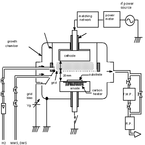
Figure 1. Schematic diagram of triode plasma CVD apparatus. 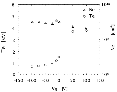
Figure 2. Variation in the electron temperature and electron density in the afterglow region measured by a double probe. Substrates were placed on an electrically floated anode. Base pressure was below 6.7x10⁻⁵ Pa in the growth chamber, which was evacuated using a turbo-molecular pump and a mechanical rotary pump. Si (100) substrates, which were thermally oxidized in dry oxygen atmosphere at 1000°C for 6 hours in an electric furnace, were used. The thickness of the SiO2 layer was about 200-300 nm. Experimental conditions are as follows: the distance between cathode and grid 20 mm, that between grid and substrate 20 mm, H2 flow rate 200 sccm, MMS and DMS gases (TRI Chem. Lab. Inc., 99.9999%) pressure during film growth 1.3x10⁻² Pa, gas feed ratio H2/(MMS or DMS) = 85, substrate temperature 500-700°C, total gas pressure during probe measurement and film growth 133 Pa, rf power 100 W. Hydrogen plasma was generated by an rf (13.56MHz) discharge during the probe measurement without MMS. The procedure of SiC growth is as follows. After evacuating the growth chamber below 10-4 Pa, the substrate temperature was raised to 300°C, which is lower than the decomposition temperature of the source gases, by a carbon heater. With the supply of H2 and MMS (or DMS), substrate temperature was rapidly raised from 300°C to growth temperature, leading to the film growth. At the same time, rf power was supplied to the cathode and the negative DC bias was added to the grid. The crystallinity, and Si-C bonding environment of SiC films were measured using an X-ray diffractometer (RIGAKU, RADIIIA; DS 1/2˚, RS 0.15mm, SS 1/2˚) and an infrared spectrophotometer (Hitachi Model 260-10). Results and Discussion Figure 3 shows the infrared (IR) transmission spectra of the SiO2/Si substrates before and after SiC growth at 600˚C for 3hrs. The spectrum of the substrate after SiC growth presents a sharp absorption peak at 795cm-1, which indicates the transverse optical (TO) phonon of stoichiometric SiC crystal [10]. The absorbance of Si-O bonds hardly changed after the film growth. In spite of the supply of high-density hydrogen radicals, oxide layer on Si substrate was hardly etched during the SiC growth by the triode plasma CVD. 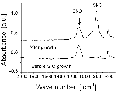
Figure 3. FTIR spectra of SiO2/Si substrates before and after SiC growth. Figure 4 shows the X-ray diffraction spectra of SiC films grown on SiO2 layer at 600°C using MMS and DMS. As can be seen in the figure, SiC (220) diffraction peak is observed in the spectrum of SiC film grown using MMS, while (111) peak is observed in that of SiC film grown using DMS. From these spectra, it was found that the SiC film grown on SiO2 layer using MMS is oriented to <110> direction. This (110) oriented SiC film is expected to possess a certain gauge factor. Therefore, the piezoresistive property of the (110) oriented SiC film was evaluated by the change of the resistance under strain using a bridge circuit. 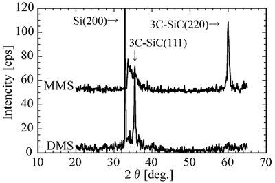
Figure 4: X-ray diffraction spectra of SiC films grown on SiO2/Si substrates using MMS and DMS as source gases. Figure 5 shows the schematic diagram of the bridge circuit for the evaluation of gauge factor of (110) oriented SiC film. RA, RB and RC are standard metal-film resistors. Rx is the SiC sample. In order to obtain the precise change of the resistance, the values of RA, RB and RC were selected to be approximately the same as that of SiC sample. Under tensile strain, the resistance of the SiC film changes from Rx to Rx +ΔR and the output voltage changes. From the change of the output voltage that of the resistance can be obtained, according to the following equation. 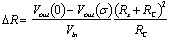 (1) (1)
where Vout(0) is the output voltage at zero strain, Vout(σ) is that at strain σ. And the gauge factor can be obtained, according to the definition.  (2) (2)
where εmax is the strain applied to the sample. If ΔR is positive, gauge factor becomes positive. 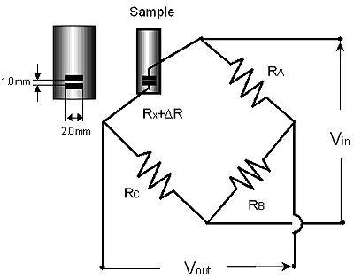
Figure 5. Schematic diagram of a bridge circuit for the evaluation of gauge factor of (110) oriented SiC film under strain. Figure 6 shows the variations in (a) the output voltage of the bridge circuit and (b) the resistance of the SiC film under the force. The strain εmax is converted from the force considering the sample sizes and the measurement conditions. The resistance decreased 0.068 percent under the tensile force of 2.9 N. From the variation in the sample resistance, the gauge factor was evaluated to –2.2. Although this value is somewhat smaller compared with that of the SiC epitaxial films[8], the improvement of the piezoresistive property will be achieved by the optimization of the growth conditions. 
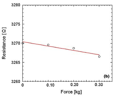
Figure 6. Variations in (a) the output voltage of a bridge circuit and (b) the resistance of (110) oriented SiC film under tensile strain. Conclusions To fabricate a SiCOI structure applicable to pressure sensors, the growth of 3C-SiC crystalline films on SiO2/Si substrates by triode plasma CVD utilizing hydrogen radicals and MMS was investigated. Under negative grid bias conditions, the (110) oriented crystal films were grown at low temperature of 600°C. From the variation in the resistance of a SiC (110) oriented film grown on SiO2 layer, gauge factor was estimated to be about -2.2. References 1. M. Mehregany, C. A. Zorman, N. Rajan and C. H. Wu, “Silicon Carbide MEMS for Harsh Environments” Proc. IEEE, Vol. 86, 1594-1610, (1998). 2. P. M. Sarro, “Silicon carbide as a new MEMS technology”, Sens. Actuators, Vol. 82, 210-218, 2000. 3. W. Reichert, E. Obermeier and J. Stoemenos, “β-SiC films on SOI substrates for high-temperature applications”, Diamond Relat. Mater., Vol. 6, 1448-1450, 1997. 4. S. Hirai, F. Jobe, M. Nakao and K. Izumi, “Study of Metamorphology Top Si Layer of SOI Wafer into 3C-SiC Using Conventional Electric Furnace”, Mater. Sci. Forum, Vol. 389-393, 347-350, 2002. 5. C. Serre, A. R. Rodriguez, A. P. Rodoriguez, J. R. Morante, L. Fonseca, M. C. Acero, R. Kogler and W. Skorupa, “β-SiC on SiO2 formed by ion implantation and bonding for micromechanics applications”, Sens. Actuators, Vol. 74, 169-173, 1999. 6. C. H. Wu, C. A. Zorman and M. Mehregany, ”Characterization of polycrystalline SiC Grown on SiO2 and Si3N4 by APCVD for MEMS Applications”, Mater. Sci. Forum, Vol. 338-342, 541-544, 2000. 7. Y. Onuma, R. Okada, H. Ono and K. Kamimura, “SiC growth on SiO2 layer by rf sputtering”, Proc. Int. Conf. SiC and Related Materials, Washington DC, USA, 1993, p.133. 8. J. S. Shor, D. Goldstein and A. D. Kurtz, “Characterization of n-Type b-SiC as a piezoresistor”, IEEE Trans. Electron Devices, Vol. 40, 1093-1099, 1993. 9. K. Yasui, K. Asada, T. Maeda and T. Akahane, “Growth of high-quality silicon carbide films on Si by triode plasma CVD using monomethylsilane”, Appl. Surf. Sci., Vol. 175-176, 495-498, 2001. 10. Y. Ohshita, “Low temperature P-Doped SiC Growth by Chemical Vapor Deposition Using CH3SiH3/PH3 Gas”, J. Electrochem. Soc., Vo. 142, 1002-1006, 1995. Contact Details |