Real-time imaging reveals how tiny structural changes inside layered nanochannels track shifts in ionic current and device behavior.
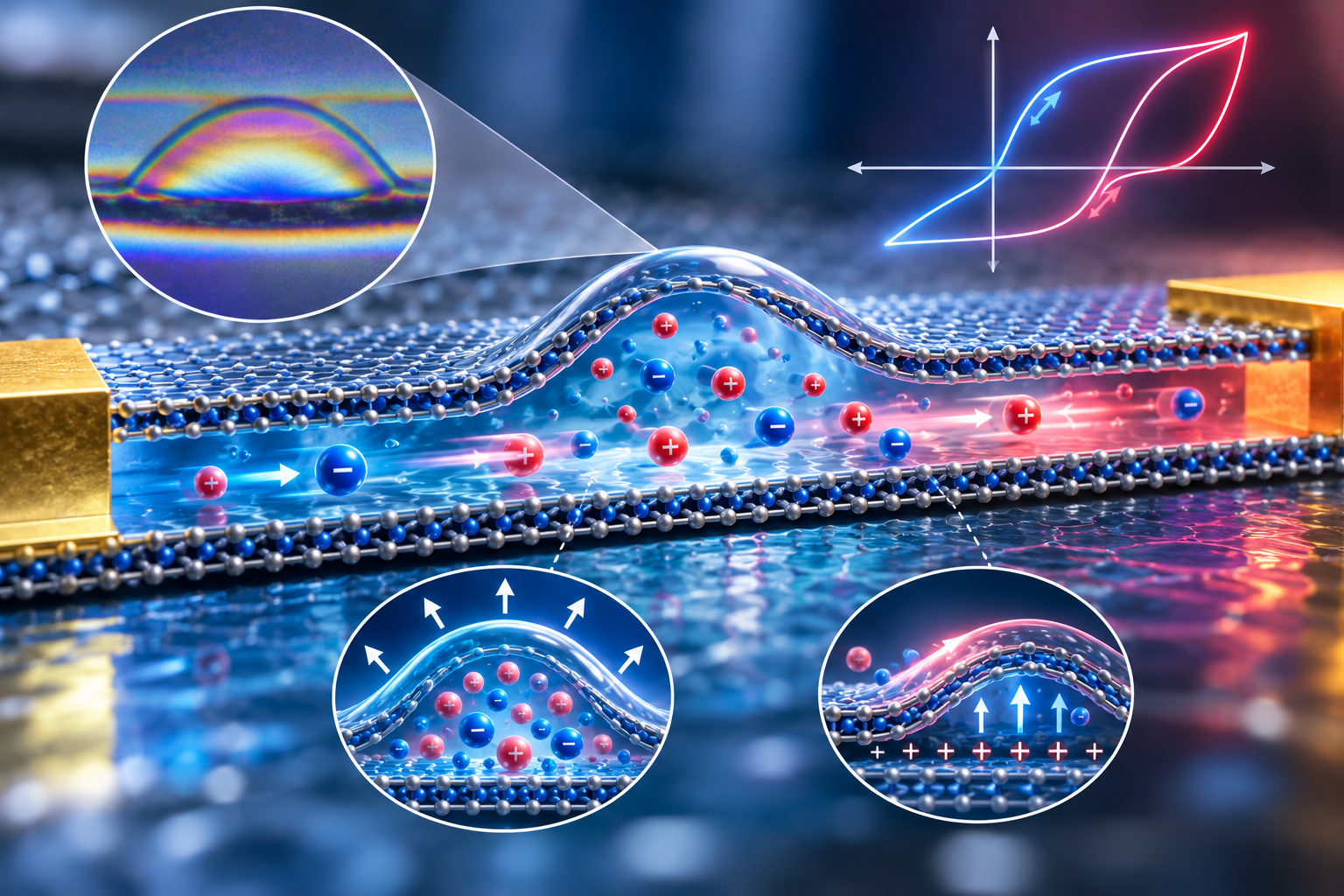
Paper: Direct imaging elucidates ionic memory in two-dimensional nanochannels. AI-generated abstract conceptual image created using ChatGPT/OpenAI
A recent study in the journal Nature Materials reveals the mechanical origin of ionic memory in two-dimensional (2D) nanochannels.
By combining optical imaging with electrical measurements, the researchers demonstrate that sufficiently large applied voltages can trigger the formation or enlargement of liquid-filled blisters that alter channel geometry and ion transport.
The results establish electromechanical coupling as a mechanism for ionic memory in the devices studied and offer new strategies for developing reliable nanofluidic memristors for ion-based information processing.
Understanding the Mechanism Behind Ionic Memory
Nanofluidic devices transport ions through extremely narrow channels, where confinement and surface interactions can produce unusual electrical behavior. Some devices allow current to flow more readily in one direction than the other, while others exhibit memristive hysteresis. The memory effect has attracted interest in neuromorphic computing, which aims to process information using principles like those of biological neural networks.
Researchers have proposed several mechanisms to explain ionic memory in two-dimensional (2D) nanochannels, including ion-specific interactions, chemical reactions, changes in wetting behavior, and mechanical deformation.
Some studies have suggested that ion pairing or polyelectrolyte formation could drive memory effects in channels assembled from layered materials. But researchers have lacked direct experimental evidence to confirm these explanations.
In this study, the researchers combined real-time optical imaging with electrical measurements to observe structural changes alongside ionic current. They identified two types of voltage-responsive blisters, which modeling linked to distinct mechanisms. These findings help explain the diverse electrical responses and evolving behavior of nominally similar nanochannel devices.
Building and Investigating Two-Dimensional Nanochannels
The researchers fabricated 2D nanochannels by stacking hexagonal boron nitride (hBN) layers around a thin graphene spacer. This arrangement created narrow channels for ion transport, with an etched aperture defining a channel length of about 5 μm. They examined 14 devices to investigate how their structures influenced electrical behavior.
The researchers combined reflection microscopy with electrical measurements in a custom fluidic system.
They used thin-film interferometry to detect changes in reflected light and identify variations in the layered structures' shape. A water-dipping objective captured images while electrodes applied a sinusoidal voltage and measured the resulting ionic current.
By synchronizing the two measurements, they tracked structural changes alongside variations in electrical conductance.
To quantify these changes, the researchers used voltage-induced contrast (VIC), which compares reflected-light intensity under an applied voltage with the intensity at zero voltage. They used optical modeling to estimate blister heights from the contrast changes, treating the converted heights as order-of-magnitude estimates because of uncertainty in layer thicknesses.
They tested aqueous potassium chloride solutions at concentrations from 1 mM to 1 M, along with 1 M solutions of sodium chloride, lithium chloride, and calcium chloride. They also developed theoretical models to assess whether osmotic pressure and electrostatic forces could overcome interfacial adhesion and deform the channel walls.
How Blister Formation Controls Ionic Conduction
The nanochannels showed a linear relationship between voltage and current at low applied voltages, with no significant voltage-induced deformation. Some devices conducted more strongly than theoretical models predicted. The researchers attributed this difference partly to pre-existing blisters and imperfect adhesion between the layered materials, which could increase the effective channel cross-section.
When the applied voltage exceeded about 0.2 V in one tested device, blisters appeared or expanded, coinciding with nonlinear conduction and electrical hysteresis. These deformations changed the channel geometry and altered ion transport. As the blisters expanded and contracted along different paths, the devices retained a memory of their electrical history.
In one device, conductance increased by 50% in less than a second after a specific blister changed shape. Another device showed distinct changes in its current-voltage curves across repeated cycles. The researchers traced these variations to two regions with evolving blisters. Stable blister behavior supported repeatable electrical responses, while unpredictable deformation caused device variability.
Two blister types emerged from their response to voltage polarity. Bidirectional blisters expanded under both positive and negative voltages. The researchers' model attributes this response to concentration polarization, which increases the average salt concentration inside the channel and creates an osmotic pressure difference between the channel and reservoir.
Unidirectional blisters responded mainly to one voltage polarity and were consistent with a model in which electrostatic forces on surface charges pushed the confining layers outward.
Analysis of 50 blisters across nine devices confirmed these distinct behaviors. Most blisters collapsed when the voltage returned to zero, but some retained their deformation during slower voltage cycles, especially at 10 to 30 mHz in one device, providing a physical basis for non-volatile ionic memory.
The study then used theoretical modeling to examine what could drive these deformations. The results indicated that osmotic and electrostatic pressures could overcome relatively weak interfacial adhesion. The models predict that different blister-growth and recession mechanics produce hysteresis in blister height and conductance, explaining how nanoscale structural changes control ionic conduction and memory.
Designing More Reliable Nanofluidic Memory Devices
The study identifies mechanical deformation as a key mechanism behind the ionic memory observed in the 2D nanochannel devices.
Applied voltage deforms the channel walls, changing the space available for ion transport. These structural changes explain electrical hysteresis, sudden conductance shifts, and variations between similar devices. The findings show that models must consider mechanical effects alongside ionic interactions to explain nanofluidic behavior.
The authors also note a limitation: purely ionic memory mechanisms that produce refractive-index changes below about 1% could fall below the optical method's detection limit, so the results do not rule out such mechanisms in systems without measurable deformation.
The study identified surface charge, interfacial adhesion, channel geometry, and driving frequency as factors that influence blister formation and memory retention. Introducing low-adhesion regions at selected locations could improve device consistency and make blister formation more reproducible in nanofluidic memristors.
Overall, the findings establish electromechanical coupling as a promising design principle for ionic memory devices. Controlling blister formation could improve nanofluidic memristor reliability and enable electrically actuated nanofluidic valves, advancing ion-based information processing technologies.
Disclaimer: The views expressed here are those of the author expressed in their private capacity and do not necessarily represent the views of AZoM.com Limited T/A AZoNetwork the owner and operator of this website. This disclaimer forms part of the Terms and conditions of use of this website.