Regular checks on coating processes are essential for manufacturers to maintain product output quality, for example the thickness of coatings. Coatings are frequently composed of costly materials and it is crucial to find a sensible and cost-effective balance between thin layers and a sufficient thickness to guarantee product quality.
Analyzing coatings or thin layers is a common undertaking in Micro-XRF spectrometry. This method is very attractive for analyzing single or multiple layers as it is both non-destructive and can use the ability of X-rays to penetrate the sample to obtain information on the sub-surface composition. The polycapillary optic of the M4 TORNADO means that an excitation spot of <20 µm can be achieved, and a layer thickness analysis with high spatial resolution is possible.
The lab report here provides a comprehensive analysis of a copper-aluminum bilayer on a glass substrate to determine the layer thickness and the Cu:Al ratio through the sample. Map results were compared with single point measurements to provide a comparison of these two analysis procedures.
Functional principle
The high photon energy of X-rays enables them to penetrate matter and induce characteristic effects such as X-ray fluorescence. The fluorescence in turn can be detected and provide a range of information on the composition of the sample.
Coated structures with sufficiently thin layers will see fluorescence produced in all layers and generally radiated back out of the sample (Fig. 1). The secondary X-rays may be detected and the ratios of the fluorescence signals from the individual layers used to calculate the thickness and the elemental composition of each individual layer.
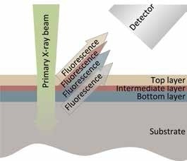
Figure 1. Functional principle of layer fluorescence
Sample
Analysis was undertaken on a sample consisting of a 5 cm x 5 cm glass substrate coated with a copper-aluminum bilayer. The sample was manufactured by a magnetron sputtering technique using a dual material target containing Cu and Al.
Measurement Conditions
The measurements were performed using a Bruker M4 TORNADO equipped with a Rh X-ray tube and a polycapillary lens. This instrument provides high spatial resolution with rapid data processing and a motorized high speed X-Y-Z stage for precise sample positioning and distribution analysis. Standard measurement conditions were used as following:
- tube voltage of 50 kV
- current of 200 µA
- no primary beam filter
- chamber pressure of 20 mbar.
Two comparatively large coated regions were examined and were separated by an uncoated area running diagonally across the sample surface. This analytical task required a spatially resolved quantitative analysis of the thin metallic layer coating.
In the Area workspace of the M4 TORNADO software, a large area image of the sample was captured using the handy Mosaic function, which can be seen in Fig. 2. A map region of 1000 x 1000 pixels (green frame) was set with a pixel size of 50 µm and a dwell time of 50 ms/pixel. To complete the measurements to the required resolution meant a total acquisition time of 15 hours.
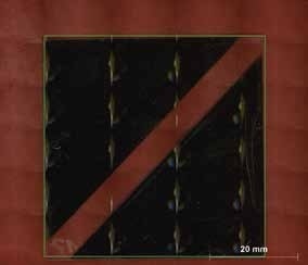
Figure 2. Mosaic sample image with defined map area
High Resolution Map Results
Fig. 3 displays the qualitative layer composition of the Cu-Al layer and Si in the glass substrate. The gradient of the Cu:Al ratio may be clearly seen. However, no layer thickness information is evident in this map. Consequently, by using the new XMethod software tool, an analysis method can be configured to determine the thickness of the metallic layer.
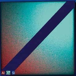
Figure 3. Elemental distribution of the Cu and Al coated glass substrate
Fig. 4a displays a false color rendering of the layer thickness map using 10 x 10 pixel binning. This marks a 500 µm spatial resolution with an overall measurement time of 5 s per binned pixel.
The radially symmetric layer thickness gradient is not centred precisely in the middle of the sample but is actually slightly offset to the right. Maximum layer thickness is determined to be 380 nm, and at the edges of the sample the minimum thickness is merely 270 nm.
Fig. 4b and 4c illustrate the false color images of the measured element signal intensities for both Cu and Al. The maximum intensity for Cu is in the top right hand corner of the sample. The greatest Al signal is found slightly shifted to the right of the bottom left hand corner.
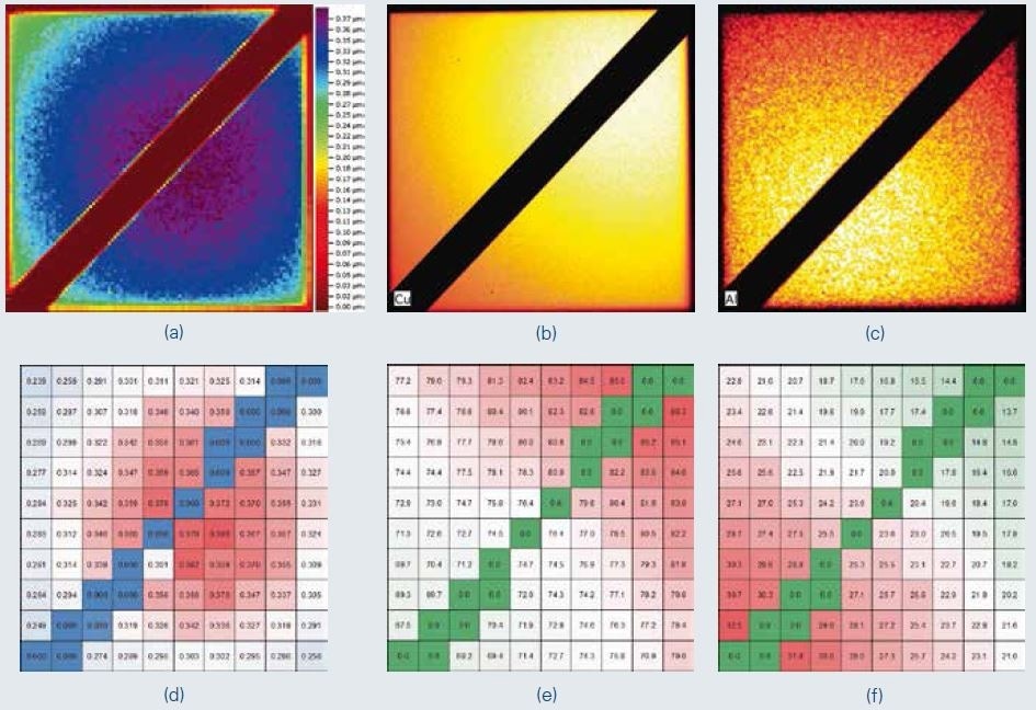
Figure 4. Area scan results. a) Quantified layer thickness along the sample, b–c) Qualitatively measured element intensity of Cu and Al, d) Quantification results of the point measurements for the layer thickness in µm, e) Mass fraction of Cu in wt.%, f) Mass fraction of Al in wt.%
Quick Multi-Point Measurement Results
As an alternative to acquiring map data for an extended time over a number of hours, a reduced number of points can be defined in a grid and analyzed for thickness separately. By using a measurement time of only 10 seconds per point across a matrix measuring 10 x 10 (Fig. 5), a quick overview of the sample’s layer thickness can be obtained in a timescale of roughly 20 minutes.
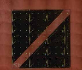
Figure 5. Mosaic sample image with defined single measurement points
By defining the measurement method/criteria in the XMethod editor and recording and quantifying the point spectra, the discrete measurement results could be conveniently exported to MS Excel® and displayed as shown in Fig. 4d–4f. The different color profiles emphasize the variation in the thickness of the layer and also the elemental composition.
The layer thickness results shown in Fig. 4d accurately match the corresponding results of the map data. The point measurement results for the Cu concentration in the layer defined in Fig. 4e indicate maximum values for the top right corner of the sample. This is in agreement with the qualitative element intensities exhibited in Fig. 3.
Fig. 4f shows the Al concentrations at 100 defined measurement points. The maximum is found in the lower left corner of the sample as expected from previous qualitative results. A decrease of the measured Al intensity may be attributed more to the lower layer thickness in this area than a variation in the element ratio. Overall the Cu:Al ratio varies from 86:14 in the top right hand corner of the sample to 67:33 in the bottom left hand corner.
Conclusion
Irrespective of the analytical methodology for full area scans and single point measurements, identical layer thickness values were seen across the sample for both procedures. This indicates that the combination of M4 TORNADO with the complimentary XMethod tool is a very useful combination to analyze and provide definitive conclusions on thin metallic layers.
It is worth mentioning that a stable quantitative fundamental parameter analysis of the Cu-Al layer is possible with spectra accumulated over just 5 s.
Higher spatial resolution is obtained at the cost of increased measurement time. However, this can be useful for samples where the layer thickness differs over relatively short distances. For carrying out quality assessment, evaluating using a coarser grid is generally adequate and certainly more time effective.
Author
Falk Reinhardt, Application Scientist Micro-XRF, Bruker Nano GmbH

This information has been sourced, reviewed and adapted from materials provided by Bruker Nano Analytics.
For more information on this source, please visit Bruker Nano Analytics.