Many reports place PIC market growth at a CAGR1 of over 20% until 2025 and even beyond. Because of this, superior automation for both assembly and testing is critical in enabling high-volume production with a feasible cost-per-part.
Photonics technology is seeing a move towards higher levels of integration, with multiple components and functions now being available within a single device or small hybrid assembly. This is known as a photonic integrated circuit (PIC).
Development has focused on meeting bandwidth density and power dissipation requirements, due to ever-increasing telecom and datacom demands (data centers for internet communications and cloud services, respectively).
Transferring data in and out effectively has become of utmost concern, much more so than absolute processing power. This has led to these sectors becoming the driving force behind the ongoing evolution of PICs.
Photonics is generally accepted as an indispensable enabling technology for a wide range of applications and industrial processes, meaning that the PIC has naturally ‘trickled over’ in to other photonics-enable dsectors and applications. This in turn has led to increased scope in the expanding infrastructure needed to support PIC ecosystems. The technology infrastructure is now deemed by many to be stable enough to be mainstreamed.
The Emerging PIC Applications
Other than telecom and datacom PIC applications, different, strong market opportunities exist which take advantage of similar IR wavelengths, benefitting from the existing development maturity at those wavelengths. A diverse array of applications also exist which have conventionally looked to use miniaturization at more visible wavelengths.
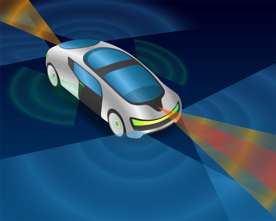
Figure 1. LiDAR and other optical sensor applications for automotive are set to grow significantly. Image Credit: pixelfit/iStock.com
One example of the former is the progressively more advanced optical sensing devices designed for (more and more autonomous) automotive applications. A growing quantity of optical sensing devices, such as LiDAR2, are being incorporated into varied automotive transport systems. This sector is expected to experience substantial upheaval3 over the next 15 to 20 years.
A number of other markets are well worth considering. These include: virtual and augmented reality applications (these are especially important when they affect consumer markets); biophotonics, OCT and biomedical sensing devices for decentralized testing (point-of-care diagnostics which make use of optofluidic and/or BioMEM devices); making more ‘sense’ of the world around us utilizing a large number of networked sensors (the Internet of Things (IoT)); and RF photonics used for terahertz technology, quantum systems, defense and aerospace, among others.
These applications all require integrated opto-electronic devices which will require high-volume manufacturing, assembly, testing and appropriate packaging if these market forecasts are accurate.

Figure 2. Augmented/virtual reality applications exhibit the volume scales that justify PIC use.
Gearing Up for High Volume
Conventionally, device production – including most photonics application spaces - is designed for volumes between hundreds and thousands of components. In the past, both photonics and microelectronics have been manufactured and integrated individually before being assembled into a complete device, tested and ultimately packaged.
However, when dealing with quantities of photonic devices in the hundreds of thousands or even millions, ‘individual’ and ‘discrete’ procedures are no longer sensible approaches.
For PIC assembly, the various active/passive functional elements must still be installed and combined (hybridized) onto a base platform. Rather than a single technology platform delivering the full range of functionality necessary, various different material systems contribute distinct functional building blocks to the PIC ecosystem.
It is imperative that these are extremely integration-capable, meaning that they can always accommodate a wafer-level approach to assembly and test. It is also beneficial to move singulation as far down the production line as is practical.
There are similarities between this and the case for CMOS, where a pathway to high-volume, wafer-scale production is enabled via a reduction in element diversity, in turn achieved by rationalizing them down to a reduced amount of reciprocally compatible micro-platforms.
Separate assembly and test methods have been satisfactory for low volumes, but are totally unworkable when considerably higher manufacturing volumes are required.
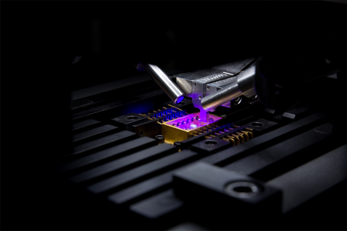
Figure 3. Discrete assembly and test approaches have been acceptable at low volumes, but are entirely unrealistic at much higher manufacturing volumes.
The transition towards increased integration of opto-electronics requires a convergence of both photonics and electronics, throughout every aspect of production (design, manufacturing, assembly, test and packaging) and not just at the component manufacturing stage.
The primary limitation of this approach is that the current development status of the PIC eco-system infrastructure is still fairly rudimentary in comparison with the maturity, scale (the number of wafers) and level of automation that are frequently seen in CMOS processes for micro-electronics production.
This convergence will take some time to occur, primarily due to the inconsistency between infrastructure maturity for PICs in contrast with CMOS, which adds up to around 40 years.
Opportunities may exist whereby knowledge gained in CMOS can be transferred directly over to PIC. The cost of assembly, testing and packaging of standard CMOS chips was reduced to the order of 10-20 % of the whole cost of production through the implementation of in-line test procedures – this is just one example of this potential for knowledge transfer.
Optical Assembly and Testing Procedures as the Bottleneck
In principle, the overarching production approach used for PICs is identical to that of conventional micro-electronics. The increase in complexity results from optical probing requirements:
- The variety of optical characteristics being measured, such as polarization or spectral properties, transmission losses, multiple (fiber) channels, and temperature sensitivity
- Assembly or probing (testing) of optical waveguides or fiber elements needs to employ sub-100 nm positioning, as opposed to 80 x 80 µm pads (or larger) required for electrical contacting
- Optical connections need to provide for high reliability, accuracy and consistency, with process time impacting substantially on overall device cycle time
These distinct requirements have two consequences, and they are inconsistent with the suggestion that CMOS knowledge can be directly transposed onto PICs.
The first consequence is that assembly processes for PICs take from a few tens of seconds to several tens of minutes to complete, placing stringent requirements on the complexity of machinery designed to accomplish these tasks. It is highly challenging to attain a satisfactorily short cycle time without endangering yield, even when considering the discrete assembly of singulated PICs into devices.
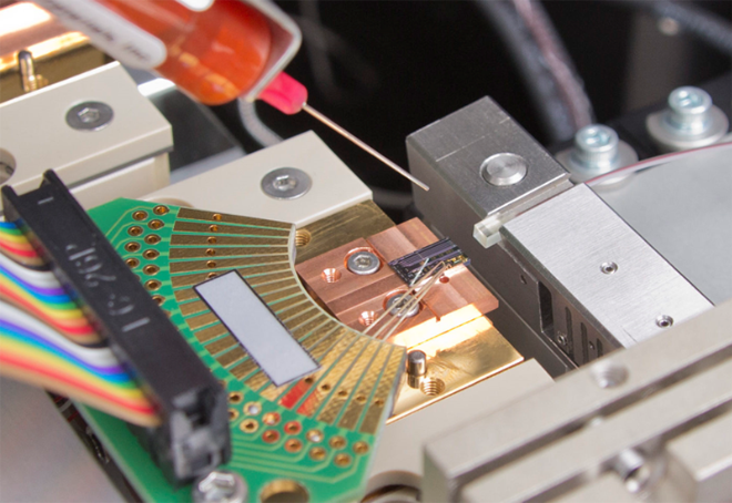
Figure 4. Coupling a fiber array to a PIC using an alignment system with 6 degrees of freedom.
The second consequence or issue is that, as PIC testing needs both electrical and optical probing, testing procedures have an added layer of complexity. Each approach to probing involves its own set of parameter-specific requirements (DC/low frequency and RF for electrical), as well as needing different positional accuracy.
To address these issues, a conventional hybrid optical/electrical probe head for PICs will generally utilize a layout that caters to the more challenging optical requirements first.
ficonTEC has been pursuing this approach in a range of initiatives and projects, and it would be very useful for the company to have the chance to explore these requirements in a genuine manufacturing setting.
While being slightly out of date, it is generally understood that PICs’4 front-end procedures only add 20 % to the total production cost, while back-end processes (assembly, packaging, and testing) contribute around 80 %.
Realistically, a pooled suite of optical and electrical testing procedures must now be explored, so it is impractical to assume congruity with CMOS in this aspect.
That said, it might be reasonably presumed that implementing recognized CMOS-style in-line test infrastructures and procedures, at least as far as possible, may help minimize these back-end costs.
Assembly and Test for Higher Volumes
A shift to wafer-level-capable processes is required because of increasing volumes. In the wafer environment, diverse optical test parameters, overall pin count and coupling type/speed/accuracy can all pose problems throughout the process chain. Additionally, thermal considerations become more relevant, as many optical features housed on a PIC either generate heat or are temperature sensitive.
Since reworking after an assembly step is almost impossible in many applications, PIC device manufacture’s specialized requirements mean that testing is an ever more central part of the assembly cycle.
Such issues can be alleviated by applying careful design principles in the development phase, specifying explicitly what must be tested, outlining when and to what level of required tests must take place, and by providing a suitable approach to probing.
Coupling is an important consideration that must be approached with care. Edge coupling provides some practical benefits,5 however, unless supplementary process steps are introduced, it is generally not accessible before dicing.
Device access at wafer level is offered by grating couplers (VGCs), with one approach including VGCs as ‘test only’ interim structures throughout manufacturing (removable optical test points).6
Another approach uses a combination of both – surface coupling is employed for wafer-level testing even when edge coupling the packaged device.
It is also important to take into consideration the characterization processes which can occur at both the module level and as a device qualification test, post-process. In-line characterization and final device testing may have varying requirements.
These procedures must also factor in any application-specific needs, such as hermiticity and/or environmental needs, which can be very different between Telcordia and biomedical applications. Finally, there could be further third-party tests that must be incorporated.
In most cases, the assembly layout and related process requirements in PIC production are dictated by optical requirements ahead of electrical I/O requirements. The full range of optical, electrical, fixturing and layout considerations should be explored as early as possible if conflicts are to be minimized later on.
Unfortunately, however, instead of addressing aspects like automated assembly or scalability, these considerations still primarily stem from immediate device-specific needs. High-volume products generally lean toward specifically tailored solutions that allow manufacturers to achieve the optimum combination of performance, size, and/or cost savings.
Experience suggests that an ‘optical first’ approach can prove more advantageous. A mix of practical ideas for the pre-alignment of optical probing, and for some degree of parallelism for wafer-level testing to be combined with optical/electrical probe approaches are required. There is, however, no real way of avoiding an increased implementation of automation.
Projects and Initiatives
ficonTEC has developed a new wafer-level tester system for AIM Photonics7. This tester came complete with robotized wafer loading - one of several parallel activities designed for a higher degree of photonics integration.
With automated test cycles for both edge couplers and vertical grating, the system has been developed to flexibly accommodate all optical and electrical testing procedures for both wafer level and singulated chips.
Another path towards the small and medium-volume production of packaged PICs is offered via a partnership with PIXAPP.8 Solutions that are being developed for four different application domains – datacom and telecom, fiber sensing, and bio-sensing – each possessing its own particular challenges around expected reliability, cost implications and packaging.
The relationship has been organized by the Tyndall National Institute in Cork, Ireland.9 PIXAPP will supply industrial users with single-point access to a comprehensive overview of the PIC supply chain, linking design tools to fully automated test, assembly and packaging systems.
ficonTEC hopes to gain an improved understanding of PIC assembly and testing needs across various market segments via this long-term work with a diverse array of partners and their specific needs.
Figure 5. Key focus areas for the PIXAPP photonics packaging pilot line. Image Credit: PIXAPP
ficonTEC has also worked with numerous high-profile leaders in global technology, collaborating on projects which currently use wafer-level processes in production. This has led to significant experience gains. The ideas and examples outlined above are mirrored by the synopses of some of these projects:
- Pioneering assembly development designed to reduce cycle time for low-cost air purity sensor devices, aimed at very high-volume automotive applications
- The use of a VGC to couple fiber onto a PIC in a medium-volume TOSA/ROSA application
- Development of custom handling systems for innovative surface connector technology which is intended to make on-chip coupling (and testing) easier
- Significant process automation development with a view to reducing process time in the assembly of silicon photonics components intended for datacom applications
ficonTEC works alongside a customer’s development teams in order to fully comprehend their needs, either working with the customer directly to develop required systems or tuning these within the available system’s framework and capabilities.
In some cases, these partnerships are already overseeing the implementation of essential process and system changes required to upscale production.
These implementations are not just seeing multiple production lines running in parallel on the same tasks, however. An additional layer of control is in place, in the form of a common revision control server. As well as system-wide updates, this allows individual process updates to be implemented automatically and remotely.
Adoption of these advanced automation procedures will soon be unavoidable for any organization transitioning to increased production numbers while simultaneously hoping to balance production costs against device sophistication.
Outlook
While there may be a number of barriers to the rapid assembly and testing of PICs, photonic device production can be enhanced via improved automation and process development. As with microelectronics, the standards that dictate the overarching ecosystem will be developed, and these standards will ultimately lead to more capable testing and assembly systems.
ficonTEC’s work in the areas of testing, assembly, and packaging for photonic devices continues to grow.
Its expertise stems from installing more than 800 systems around the world since 2001. This experience has also shown that even now, requests for new systems almost exclusively include very distinct requirements.
The central theme in the development of all of these systems has been the appropriately timed design of the production process, taking into account the range of tools available.
References and Further Reading
- Examples of market researchers predicting substantial PIC market growth potential: https://bit.ly/2k8vJ2q, https://bit.ly/2k5OYK1, and https://bit.ly/2wRMzvX
- LiDAR Technology: https://bit.ly/2IWZTVp
- Automotive sector volatility and growth potential
- PIC roadmap example: JEPPIX Roadmap 2018, p.37
- ‘Wafer-scale high-density edge coupling for high throughput testing of silicon photonics’, R. Polster, et al, OFC 2018 – see also AIM Photonics
- ‘Towards autonomous testing of photonic integrated circuits’, M. Milosevic, Proc. SPIE 10108, Silicon Photonics XII, 1010817 (2017/02/20)
- Link to Aim Photonics: http://www.aimphotonics.com/
- Link to PIXAPP: https://pixapp.eu/
- Link to Tyndall National Institute: https://www.tyndall.ie/about-us
- Link to Euratom EU Horizon 2020 program information: https://research-and-innovation.ec.europa.eu/funding/funding-opportunities/funding-programmes-and-open-calls/horizon-2020_en
- Link to EMVA program information: http://www.emva.org/

This information has been sourced, reviewed and adapted from materials provided by ficonTEC Service GmbH.
For more information on this source, please visit ficonTEC Service GmbH.