Recent years have seen a revolution in the semiconductor industry. Common, longstanding practices involving increases in transistor density and performance-per-watt improvements (illustrated by Moore’s law and Dennard scaling) are beginning to encounter fundamental physical limitations.
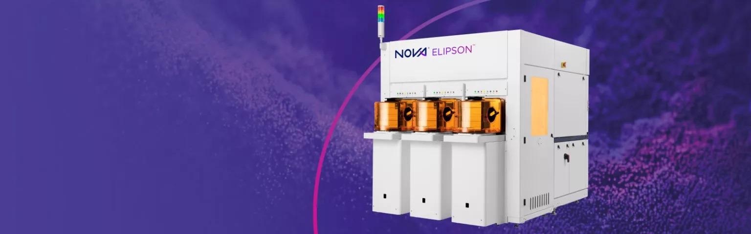
Image Credit: Nova Measuring Instruments Ltd
This crisis has prompted a burst of innovation, resulting in revolutionary new methods of semiconductor design and operating principles that are opening up new approaches to performance enhancement.1
A central factor in this transformation has been the utilization of new materials, new compounds and new methods of control over material properties as a core consideration in device design. Using and manipulating novel materials requires suitably robust analytical and metrological techniques for process control, however.
Raman spectroscopy is one prevalent technique that is already widely regarded as a high-end metrology solution in the pharmaceutical and petrochemical industries, highly suited for both qualitative and quantitative analysis.2
Despite this recognition, uptake of Raman spectroscopy in the semiconductor industry has thus far been primarily limited to laboratory applications.
There have been technological advancements in every key component employed in this approach, for example, high-end filters, ultra-stable laser sources and low-noise detectors. These advancements have led to this 90-year-old method becoming a promising, flexible metrology technique suitable for use in high-volume semiconductor fabrication.
Raman Spectroscopy
By using Raman spectroscopy (RS), it is possible to determine the vibrational structure of molecules and materials in a non-destructive fashion. Analysis is facilitated by measuring the energies of inelastically scattered light from the sample of interest.
Raman-active materials will demonstrate a characteristic ‘fingerprint’ as part of their Raman spectrum. This fingerprint can be used to identify them as well as enabling the study of their physical properties. Different molecular structures and crystal phases generally result in totally distinct Raman spectra, enabling easy identification and differentiation.
RS is suited to an extremely diverse range of material characterization tasks, for example, stress/strain measurements, residue detection, defectivity, composition and activated doping levels.
This technology is not easy to adapt for in-line, high-volume manufacturing (HVM), however. RS is generally slow, requiring regular calibrations. It is also prone to being impacted by environmental conditions such as temperature fluctuations or acoustic and vibrational noise.
These issues can be effectively mitigated by using the NOVA ELIPSON™ - an instrument that offers rapid, ultra-stable, self-calibrated and fully automatized RS-based metrology.
NOVA ELIPSON ™ for In-line Raman Measurements
At its core, the NOVA ELIPSON™4 is a high specification, in-line metrology tool. The instrument successfully bridges the chasm between lab and fab metrology, making Raman Spectroscopy applicable to high volume manufacturing.
The NOVA ELIPSON™ combines a number of unique design features, each designed to offer accurate, flexible measuring capabilities that can be adapted to monitor a wide range of material properties, whether the application in question involves R&D or HVM.5
The platform can accommodate a number of excitation wavelengths, ranging from the UV to the visible. It also offers diagnostics capable of continually monitoring laser power and output wavelength. The laser is coupled into the system using a high-precision fiber-dock station, meaning that on-site servicing is quick and straightforward.
This combination of multiple wavelengths allows the NOVA ELIPSON™ to generate Z-sensitive profiles of a range of material properties, for example, vertical strain distribution, poly Si crystallinity and grain size along high aspect ratio geometries.
A notable challenge when undertaking Raman measurements is that the scattered signal is very weak. The wavelength of the Raman signal also tends to be particularly close to the exciting laser line, meaning that efficiently filtering out the laser line and preventing this from reaching the detector poses a significant challenge.
The NOVA ELIPSON™ has been specifically designed and built to address these challenges, providing rapid Raman detection at a broad detection range for every excitation wavelength.
The tool has also been designed to offer seamless, automatic, ongoing calibration protocols, allowing it to satisfy the strict precision requirements of the fab environment.
Where applications require spatially-resolved measurements (such as when mapping local regions), the NOVA ELIPSON™ can be utilized for Raman microscopy with a sub-micron spatial resolution. Localized properties (for example, those within a single region of a memory cell) may be identified, providing valuable spectral information for process control.
The Future of Fab Material Metrology
Fab in-line HVM metrology solutions have historically focused on dimensional characterization. As materials used in the fabrication process become more diverse and complex, therefore requiring more nuanced control over their properties, material metrology and process control are becoming more and more prevalent.
This increasingly diverse range of applications has generated an equally diverse set of metrology needs. The NOVA ELIPSON™ is the ideal solution to meet these needs, offering a rapid, flexible, non-destructive, fully-automatized solution.
The NOVA ELIPSON™ offers a range of proven has high-end characterization capabilities suitable for a diverse array of use cases. These use cases have included logic applications, for example, effectively characterizing stress\strain, active doping, composition, defectivity and material residue identification via the transistor module.
The memory market also features a similarly broad set of applications, for example, characterizing crystal phases, induced strain, distinguishing between amorphous, poly-crystalline or crystalline Si and determining phase in emerging memory materials.
As the NOVA ELIPSON™ proliferates into the market and becomes more commonplace, further use cases continue to be identified and developed. Each use case and new market segment further extends the potential applicability of RS for fab metrology.
References
- Lambrechts, W., Sinha, S., Abdallah, J. A., & Prinsloo, J. (2018). Extending Moore’s Law through Advanced Semiconductor Design and Processing Techniques. CRC Press.
- Paudel, A., Raijada, D., & Rantanen, J. (2015). Raman spectroscopy in pharmaceutical product design. Advanced Drug Delivery Reviews, 89, 3–20. https://doi.org/10.1016/j.addr.2015.04.003
- Khatibi, S., Ostadhassan, M., & Aghjanpour, A. (2018). Raman spectroscopy : an analytical tool for evaluating organic matter Raman spectroscopy : an analytical tool for evaluating organic matter. Journal of Oil, Gas and Petrochemical Sciences, 2(1), 00007. https://doi.org/10.30881/jogps.00007
- NOVA ELIPSON, Nova, (2021), https://www.novami.com/nova-product/nova-elipson/, accessed 20th January 2021
- Schmidt, D., Cepler, A., Oren, Y., & Fishman, D. (2021). In-line Raman spectroscopy for stacked nanosheet device manufacturing. Proceedings Volume 11611, Metrology, Inspection, and Process Control for Semiconductor Manufacturing XXXV;116111T 2021) https://doi.org/10.1117/12.2582181

This information has been sourced, reviewed and adapted from materials provided by Nova Measuring Instruments Ltd .
For more information on this source, please visit Nova Measuring Instruments Ltd .