This article discusses the role of the depletion region in a semiconductor p-n junction and the effects of doping concentration on the depletion width.
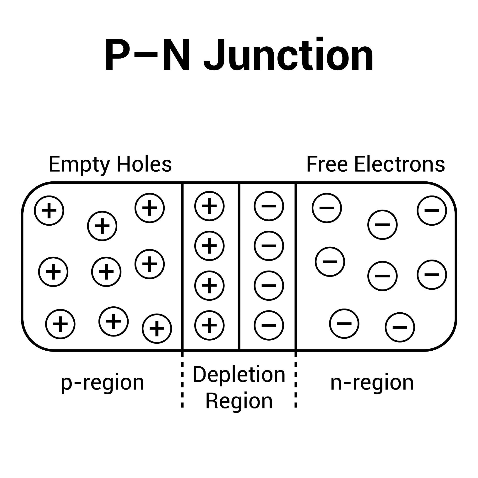
Image Credit: zizou7/Shutterstock.com
Depletion Region in a Semiconductor PN Junction
A p-n junction is an interface or boundary between p-type and n-type semiconductor materials within a single semiconductor crystal. The positive (p) side contains excess holes, while the negative (n) side contains excess electrons in the outer shells of the electrically neutral atoms, which allows only the unidirectional flow of electrical current through the p-n junction.
In semiconductors, the p-n junction is formed through the diffusion of dopants, ion implantation, or epitaxy. Epitaxy involves growing a crystal-doped layer with one dopant type on top of a crystal-doped layer of another dopant type.
Ion implantation or diffusion of one type of impurity into the background of the opposite type of impurity leads to the majority of the donor impurity in one region and acceptor impurity ions in the other region.
During charge carrier diffusion across the p-n junction due to a large carrier concentration gradient at the junction, the holes from the p-side diffuse to the n-side of the junction, leaving behind negatively charged acceptor ions, while electrons from the n-side diffuse to the p-side, leaving behind the positively charged donor ions.
Subsequently, a space charge is formed due to the presence of negatively charged acceptor ions in the p-type region and positively charged donor ions in the n-type region near the junction.
A potential barrier/difference is developed as the space charge region leads to the creation of an electric field, which prevents further diffusion of charge carriers across the junction. Thus, the net flow of carriers becomes zero and a state of electrostatic equilibrium is realized across the p-n junction.
The space charge region on the two junction sides is referred to as the depletion region/transition region due to the lack of free charge carriers in the region. Depletion width is the sum of depletion region boundaries on the p-region side and n-region side.
The region outside the depletion width on both sides of the junction is referred to as a quasi-neutral region/bulk region/ohmic region as the majority carrier distribution in this region does not significantly differ from the impurity distribution.
Effects of Doping Concentration on the Depletion Width
The depletion region width on each side of the p-n junction inversely varies with the dopant concentration. Thus, the depletion width decreases when the dopant concentration is higher and increases when the dopant concentration is lower.
In one-sided step junctions, the dopant concentration on one side of the junction remains much higher compared to the other side. Thus, the depletion width in one-sided step junctions expands entirely into the lighter-doped side.
In lightly doped semiconductors, the free electrons from the n-side fill the holes in the atoms at the p-side by crossing the junction before they recombine with the n-side positive ions due to an extremely slow recombination rate. Thus, the atom at the p-side becomes a negative ion by gaining an extra electron.
Similarly, the holes from the p-side also cross the junction and occupy the place of electrons at the n-side before recombining with the p-side negative ions. Thus the atom at the n-side becomes a positive ion by losing the valence electron.
The mechanism gradually increases the negative ions at the p-side and positive ions at the n-side, which increases the width of the depletion region over time in lightly doped semiconductors.
Studies on Depletion Region in Semiconductor PN Junctions
Gallium nitride (GaN) is a wide bandgap semiconductor used in the fabrication of energy-efficient white light-emitting diodes and power electronic devices. In a study published in the Journal of Applied Physics, researchers determined the effect of the deep acceptor/magnesium (Mg) on the band bending within the depletion region of GaN semiconductors.
Specifically, the depletion/transition region width that separates the mobile holes from the space charge edge was thoroughly investigated. The deep nature of the Mg acceptor can significantly influence the performance of high-speed GaN-based bipolar devices.
High-frequency modulation of the depletion region was discussed for both the small- and large-signal cases. Calculated results were compared to the experimental frequency-dependent capacitance measurements performed on Mg-doped GaN samples for the small signal case.
The results demonstrated that the depletion region form was similar to the case of a material doped with both deep traps and shallow dopants. Dispersion effects were attributed to the time required for the dopant/Mg acceptor to change ionization states.
However, the extent of dispersion was difficult to calculate in large-signal high-frequency modulation. Dispersion effects in small-signal capacitance were used to characterize the depletion region. Reduced dopant/Mg acceptor density was observed near the p-n junction due to the memory effect in metal-organic chemical vapor deposition growth of Mg-doped GaN.
More from AZoM: How Does Doping Affect the Conductivity of a Semiconductor?
References and Further Reading
Arora, N. (1993). Review of Basic Semiconductor and pn Junction Theory. In: MOSFET Models for VLSI Circuit Simulation. Computational Microelectronics. https://doi.org/10.1007/978-3-7091-9247-4_2
Kozodoy, P., Denbaars, S. P., Mishra, U.K.. (2000). Depletion region effects in Mg-doped GaN. Journal of Applied Physics. 87, 770-775. https://www.researchgate.net/publication/234904996_Depletion_region_effects_in_Mg-doped_GaN
Hilsum, C. (1979). Semiconductors (2nd edn). Physics Bulletin, 30, 528. https://iopscience.iop.org/article/10.1088/0031-9112/30/12/049/meta
Disclaimer: The views expressed here are those of the author expressed in their private capacity and do not necessarily represent the views of AZoM.com Limited T/A AZoNetwork the owner and operator of this website. This disclaimer forms part of the Terms and conditions of use of this website.