Semiconductor packaging is the engineering stage that transforms a completed silicon die into a functional electronic component. The packaging provides environmental shielding, distributes electrical signals from microscopic bond pads to outer connections, and withstands the stresses that arise during molding, soldering, and operation.
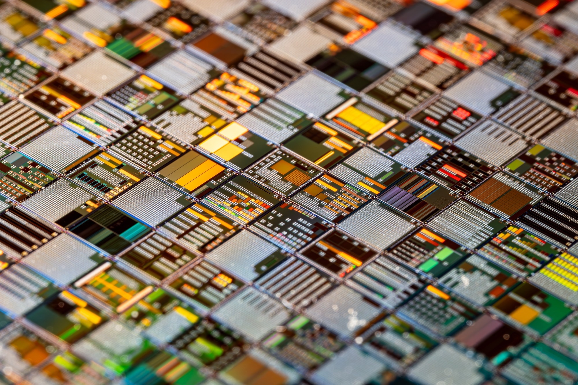
Image Credit: Andrei Armiagov/Shutterstock.com
Polyimides are essential to this process, as they reside in the thin-film interface between the device and the package, where insulation, adhesion, pattern definition, and stress control must operate simultaneously.
Following wafer production, the active die contains sensitive metallization and passivation features that may be susceptible to ionic contamination, moisture, handling damage, and stress from the assembly process.
Adding a polyimide overcoat can provide an additional protective layer on the inorganic passivation stack. Openings are formed exclusively where electrical access is required, including at bump locations or bond pads.
The objective is not merely to endure elevated temperatures. Instead, the film must maintain adherence to the chip surface while withstanding chemical treatment, curing, encapsulation, and subsequent thermal cycling.
Cracking, delamination, or excessive stress in the coating may expose interconnects or concentrate stresses at sensitive locations. For this reason, packaging formulations are developed around adhesion, residual stress, moisture behavior, and compatibility with nearby metals and dielectrics.1
While a silicon die remains relatively rigid, organic substrates, copper wiring, solder, and epoxy molding compounds exhibit different responses as temperature fluctuates. This mismatch can create concentrated strain close to metal pads and package interconnects.
In flip-chip structures, polyimides can act as a compliant stress-buffer layer that mitigates these local stresses before they harm the die-level passivation or interconnect system.
This buffering function is vital during solder reflow and reliability assessment, when repeated heating and cooling challenge interfaces throughout the package. Consequently, polyimides enhance reliability not by replacing the structural components of the package, but by managing the mechanical consequences of combining dissimilar materials.
Polyimide is also extensively used in redistribution layers (RDLs). An RDL is a thin-film wiring structure that relocates a chip’s input/output connections from its original pad arrangement to locations appropriate for bumps, balls, copper pillars, or other package interconnects. Polyimide films function as the electrically insulating foundation around and between these patterned metal lines.2
By adopting this strategy, package engineers can better utilize the die surface and connect chips in configurations that would not be practical using perimeter wire bonds alone. This makes RDL structures essential for wafer-level and fan-out packaging, where high interconnect counts and compact dimensions are required.
Furthermore, the dielectric material impacts electrical behavior, as its dielectric characteristics influence signal transmission in high-speed package wiring.3
Photosensitive polyimides offer a processing advantage. Rather than applying a polymer film and subsequently using a separate resist-and-etch workflow to define openings, a photosensitive formulation can be exposed and developed directly to form pad openings or vias before the final curing step.2
This can lower process complexity while ensuring accurate positioning of characteristics in multilayer routing architectures. In advanced packages, such patternability is just as valuable as bulk thermal stability: the material must be manufacturable at fine dimensions and remain dependable after downstream metallization, curing, bumping, and assembly operations.4
Polyimides are best viewed as custom-engineered packaging dielectrics instead of generic high-temperature polymers. Their performance can be tailored by adjusting the selection of dianhydrides, diamines, additives, and, where required, photosensitive functionality.
For instance, Benzophenonetetracarboxylic dianhydride (BTDA®) can produce polyimides with high thermal resistance, beneficial mechanical features, and reliable adhesion, making it ideal for protective coatings and stress-buffer applications.
Pairing BTDA with a suitable diamine allows formulators to balance dimensional stability, residual stress, dielectric behavior, and processability for specific package requirements.
Thanks to this molecular-level control, polyimide films are able to protect the die, insulate metal routing, accommodate assembly stress, and support fine-pitch redistribution layers in increasingly complex semiconductor packages.1,2
References and Further Reading
- 360iResearch (2025). Mastering Heat: Polyimide Films' Impact on Semiconductor Evolution. Available at: https://www.linkedin.com/pulse/mastering-heat-polyimide-films-impact-semiconductor-evolution-gvk3f.
- https://www.jommpublish.org/static/publish/BB/FC/A2/1C1DF249A983A56C4292F587D6/10.33079.jomm.25112701.pdf.
- Semiconductor Digest (2026). Polyimide for Flip Chip Packaging. Available at: https://sst.semiconductor-digest.com/2002/02/polyimide-for-flip-chip-packaging/.
- Halocarbon (2020). Photosensitive Polyimides – Critical for Advanced Semiconductor Packaging. Available at: https://www.halocarbon.com/photosensitive-polyimides-critical-for-advanced-semiconductor-packaging/.

This information has been sourced, reviewed, and adapted from materials provided by Jayhawk Fine Chemicals Corporation.
For more information on this source, please visit Jayhawk Fine Chemicals Corporation.