For modern optoelectronics, p-type transparent semiconductors with high hole mobility and regulated hole concentration are essential. However, it is very difficult to obtain transparent p-type semiconductors with the requisite optoelectrical characteristics.
Therefore, it is highly desirable to find p-type transparent materials with a high valence band maximum (VBM) position and a wide VB dispersion. p-type transparent copper iodide (CuI), which has a broad direct bandgap and a sizable exciton binding energy, has recently come under more and more scrutiny. CuI's p-type conductivity can be further increased by using the proper extrinsic acceptor doping.
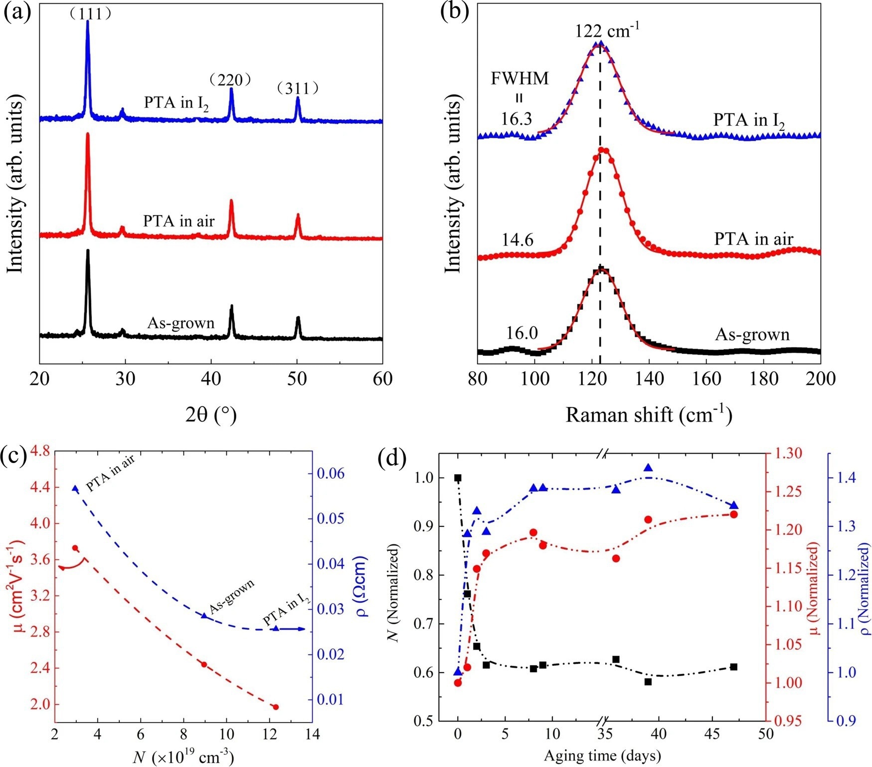
Structural and electrical properties. GIXRD spectra (a) and Raman spectra (b) of CuI thin films with different treatments, namely, as-grown (black), PTA in air (red), and PTA in iodine vapors (blue). The red lines in b are the corresponding peak fits. c Electrical properties of CuI thin films with different treatments (i.e., as-grown, PTA in air, PTA in I2). d Normalized electrical properties of as-grown CuI thin films (on glass substrate) with increasing aging time. In c or d, the black square, red circle and blue triangle denote the N, μ and ρ, respectively, and the corresponding dash lines as guides for eye. Image Credit: Li, Z et al., Nature Communications
Excitonic transitions dominate the optical characteristics of CuI in the low excitation density range. It is well known that ultrafast carrier dynamics govern semiconductors' optical characteristics and electronic transport. In other words, the relaxation, production, and trapping/recombination processes of the charged carriers involved have a significant impact on the performance of optoelectronic devices. Therefore, it is essential to comprehend these extremely fast transient processes to improve the functionality and design of various optoelectronic devices. CuI has received a lot of attention for its characterization and potential uses in devices, but the ultrafast carrier dynamics in CuI, which are strongly related to the defects, have received far less attention.
About the Study
In this study, the authors used a synergistic strategy and a variety of analytical tools to investigate the essential characteristics of copper iodide thin films. The emission at about 420 nm resulted from the recombination of electrons with neutral copper vacancies, according to steady-state photoluminescence (PL) spectra. Using femtosecond transient absorption spectroscopy, the ultrafast physical processes dependent on photogenerated carrier density were clarified.
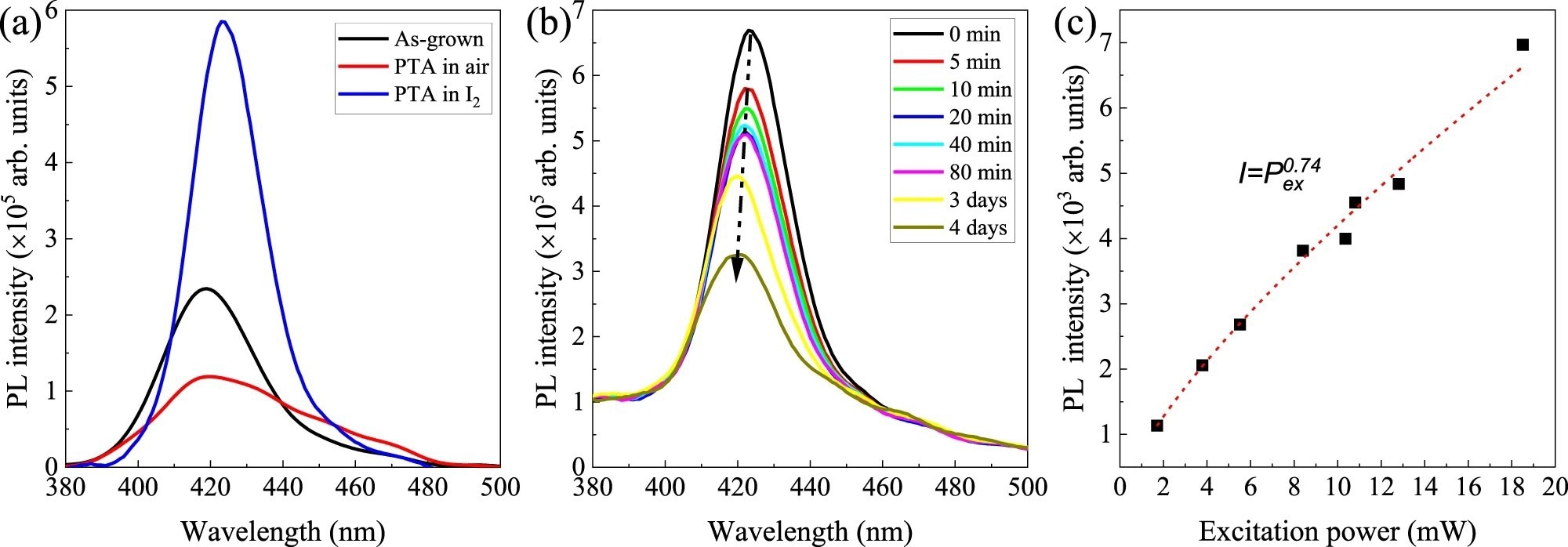
Steady-state PL emissions. a Steady-state PL spectra of CuI thin films with different treatments, i.e., as-grown (black), PTA in air (red) and PTA in I2 vapor (blue). b PL intensity of as-grown CuI thin film with different aging time in ambient air. c Excitation power (Pex)-dependent PL intensity of as-grown CuI thin film, with the fits denoted as the red dashed line. Image Credit: Li, Z et al., Nature Communications
The team demonstrated that in the event of high excitation density, the hot-carrier cooling rate was greatly slowed down by the effects of the hot-phonon bottleneck and the Auger heating. Investigations were conducted on the impact of defects on carrier recombination and two-photon-induced ultrafast carrier dynamics. These results were essential for copper iodide's optoelectronic applications.
The researchers used a variety of analytical techniques, such as Hall-effect measurements, PL spectroscopy, spectroscopic ellipsometry (SE), and femtosecond transient absorption (fs-TA) spectroscopy, to investigate the ultrafast carrier dynamics and optoelectronic properties of CuI thin films. Cu3N thin films were iodized to create the p-type transparent CuI thin films. To understand the related time scales and the mechanisms behind these ultrafast processes, the effects of excitation density and defects on carrier dynamics, such as thermalization, recombination, cooling, etc., were examined.
Observations
The as-grown CuI thin film had a hole concentration N of 9 x 1019 cm-3, but following post-growth thermal annealing (PTA) in the air (I2), the N drops increased to 3 x 1019 cm-3. The shallow native acceptors in the CuI thin films could be principally blamed for the open holes. The production of native donor defects, such as Cui, VI, and VI + Cui defect clusters, was facilitated by PTA treatments in the air. Due to the potential generation of Mahan excitons at room temperature, the absorption spectra showed that the excitonic feature of CuI persisted at a high carrier density of up to 5 x 1019 cm-3.
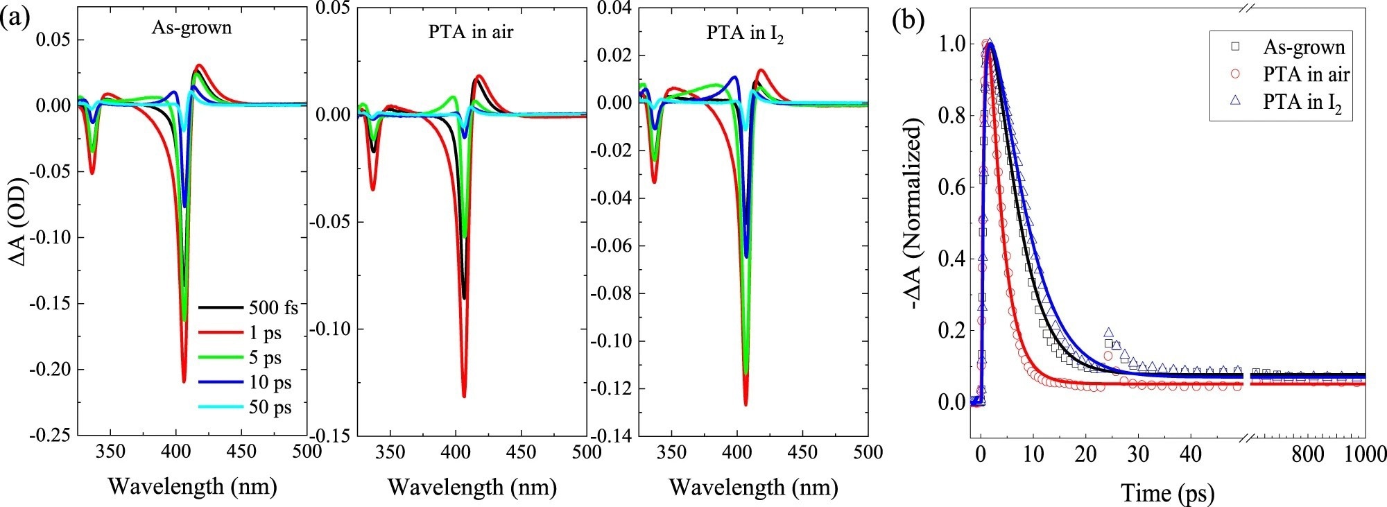
Dependence of ultrafast carrier dynamics on defects. a TA spectra of CuI thin films with different treatments (Fp = 2.54 mJ/cm2, λp = 320 nm). b Normalized PB dynamics probed at the 406 nm, with the lines the corresponding fits. Image Credit: Li, Z et al., Nature Communications
According to PL measurements, the radiative recombination was responsible for the emission peak at 420 nm. Within the time resolution of the proposed TA setup, a quasi-equilibrium distribution of photogenerated carriers was quickly formed in less than 200 fs through carrier-carrier scattering. The e-h plasmas (EHP) underwent a fast Auger recombination for relatively high excitation density greater than 1019 cm-3, with an Auger recombination coefficient of 7.42 x 10⁻³⁰ cm6/s in the decay process, with a time delay of less than 5–6 ps, while the cooling rate of the carrier with a cooling time of 6 ns noticeably slowed down due to the effects of the hot-phonon bottleneck and the Auger heating. A re-excitation was also observed at a time delay of 25 ps.
The photogenerated carriers rapidly cooled down with a cooling time of fewer than 3 ps, like the medium excitation density of 1018–1019 cm-3, and the first recombination was controlled by the trap-assisted Shockley-Read-Hall (SRH) process with an SRH recombination coefficient of 2.42 x10¹¹ s-1. The radiative exciton recombination, which had a recombination coefficient of 6.4 x 10¹⁰ s-1, occurred next at a time delay in the range of 6–20 ps when the excitation density was relatively low. The SRH recombination played the primary role in the initial decay process with a time delay of less than 6 ps.
The radiative bimolecular recombination process with a recombination coefficient of 1.3 x 10⁻¹¹ cm3 s-1 dominated the recombination kinetics since the time delay was more than 20 ps. Recombination coefficients related to the bimolecular recombination, SRH recombination, and Auger recombination dropped as excess carrier density rises; however, the radiative exciton recombination coefficient was essentially constant.
CuI thin films with various PTA treatments exhibited defect-related recombination behaviors, i.e., the radiative recombination in CuI thin film in I2 was more effective due to its higher density of V0Cu, while the nonradiative recombination in CuI thin film PTA in the air was accelerated by deep defects through the trap-assisted Auger recombination.
Conclusions
In conclusion, this study thoroughly examined CuI thin films' ultrafast carrier dynamics and optoelectronic characteristics. Measurements of fs-TA were made to comprehend the ultrafast carrier dynamics in the prepared CuI thin films. The fs-TA measurements and the Z-scan measurements were used to confirm that the CuI thin films exhibited two-photon absorption. The two-photon-generated ultrafast carrier dynamics were also discussed.
References
Li, Z. H., He, J. X., Lv, X. H., et al. Optoelectronic properties and ultrafast carrier dynamics of copper iodide thin films. Nature Communications, 13, 6346 (2022). https://www.nature.com/articles/s41467-022-34117-8
Disclaimer: The views expressed here are those of the author expressed in their private capacity and do not necessarily represent the views of AZoM.com Limited T/A AZoNetwork the owner and operator of this website. This disclaimer forms part of the Terms and conditions of use of this website.