The modular design of the WITec microscope series facilitates the integration of a time correlated single photon counting module to the alpha300 or alpha500 confocal microscope series. This enables performing various spatial and time-resolved measurements, including electro- and photoluminescence decay imaging and fluorescence lifetime imaging. This article discusses spatially resolved µElectroluminescence (µEL) analyses of a blue LED.
Spatially and Time-Resolved Electro- and Photoluminescence
Spatially resolved electro- and photoluminescence measurements (µEL and µPL) are the standard methods used for characterizing optoelectronic devices. These techniques are used to improve the performance of optoelectronic devices during the development stage and to maintain their quality during process control. Moreover, they are crucial during lifetime and failure analyses.
µEL and µPL determine the luminescence decay spectrally and spatially resolved via a microscope objective. However, the luminescence is excited by a bias voltage in µEL, but by a laser in µPL. The final (hyper-spectral) dataset consists of spectral and spatial information that can be investigated in many different ways.
Furthermore, the hyper-spectral data set will further be expanded by the variation of external parameters. Measuring the luminescence decay subsequent to a short optical or electrical excitation facilitates the analysis of dynamic properties of an optoelectronic device.
Measurement Set-up and Sample
Figure 1 illustrates the µEL measurement set-up involving an alpha300 microscope equipped with a time-correlated single photon counting (TCSPC) module for time-resolved measurements. A pulse generator (HP 8082A) was employed to create a short electrical pulse for exciting the LED emission. A high numerical aperture (NA) objective (60x, NA= 0.7) was used to collect the light emitted from the LED.
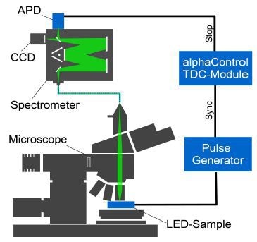
Figure 1. Micro electroluminescence setup based on an alpha300 for time resolved luminescence measurements.
The image generated by the objective was projected onto a multi-mode optical fiber (25µm diameter, NA=0.12). The light was collected by the fiber from a single point (0.42µm diameter, almost diffraction limited) of the LED and directed to a spectrometer coupled with a single photon counting detector and BI-CCD camera. The sample was scanned relating to the detection fiber using a piezo-electric scan stage.
Full luminescence spectra at every sample position were acquired by the CCD detector and the time resolved luminescence decay at selected spectral positions was measured by the single photon counting APD. To achieve this, the NIM output of the APD (MPD PDM1CTC) was linked to a time-to-digital converter (TDC) extension board in the alphaControl microscope controller. This extension board quantifies the duration between the excitation pulse and the arrival of a luminescence photon at the APD. A histogram of these arrival times provides the luminescence decay curve.
This set-up was used to analyze a commercial blue/green LED based on InGaN III-V-compound semiconductors. A microscope image of a blue LED at low magnification is depicted in Figure 2, clearly revealing the inhomogeneous distribution of the emission spectrum.
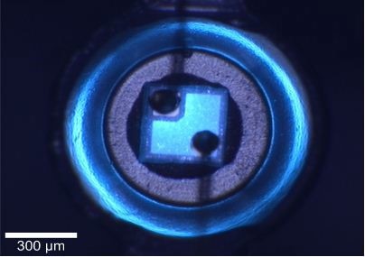
Figure 2. Video image of blue InGaN LED.
Micro-Electroluminescence Measurement
The variation of the emission spectra can be quantified with a µEL measurement at higher resolution. Inhomogeneous broadening is readily apparent in each spectrum, which is indeed a local spectrum from a small region of the sample. Hence, the emission spectra were fitted using a Gaussian curve (Figure 3). Figure 3a illustrates the average spectrum of image scan shown in Figure 4 together with Gaussian fit curve and Figure 3b displays a single spectrum of image scan shown in Figure 4 along with Gaussian fit curve.
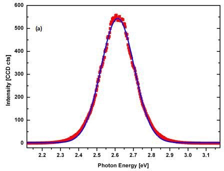
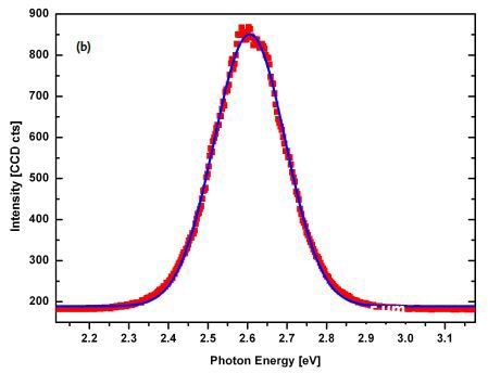
Figure 3. Gaussian curve fit of the emission spectra.
The region between the two bond pads is delineated in Figure 4. A Gaussian curve was fitted to the spectra the deliver the spectral width, spectral position and intensity of each spectrum. Figure 4a shows the intensity and Figure 4b shows the spectral center, whereas Figure 4c illustrates the spectral width.
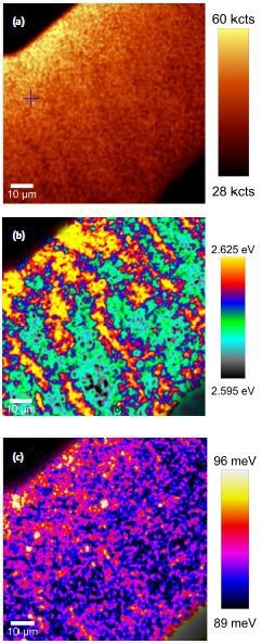
Figure 4. µEL measurement at the region between the two bond pads on the LED.
Time-Resolved Emission Spectroscopy (Total Area)
The use of a TDC extension board enables measuring the temporal decay of the emission at various wavelengths. Figure 5 displays three different time spectra at photon emission energies of 2.756eV, 2.611eV and 2.480eV, respectively. These time spectra are far from single exponential owing to the inhomogeneous distribution of gallium and indium.
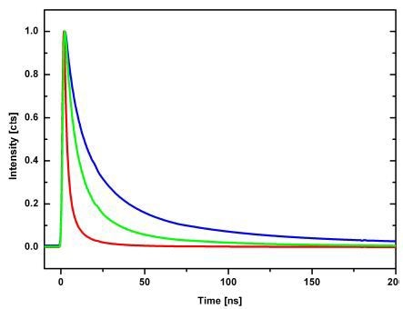
Figure 5. Time spectra at 450nm <=> 2.756eV (red), 475nm <=> 2.611eV (green) and 500nm <=> 2.480eV (blue)
Direction recombination related to light emission is possible with electrons and holes with higher energies, which can also relax into lower energy states due to indium rich clusters. Since, the decay times and populations for these relaxation channels are different, the temporal decay appears like a stretched exponential function. An average relaxation time can be obtained by evaluating the full width at half maximum (FWHM) of the emission time spectra. Figure 6 depicts the plot of the relaxation time versus photon emission energy, showing the strongest decrease of the relaxation time at the maximum of the emission spectrum.
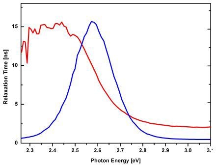
Figure 6. Relaxation time (red) and intensity (blue) vs. photon energy.
Time-Resolved Emission Spectroscopy (Local)
Besides being a function of photon energy, the relaxation time varies also locally. The same set-up can be used to collect spatially-resolved time spectra at fixed wavelengths rather than emission spectra. These time spectra were then used to calculate a map of local relaxation times. Figures 7a, 7b, and 7c delineate the spatially varying relaxation times at photon emission energies of 2.756eV (450nm), 2.611eV (475nm) and 2.480eV (500nm), respectively.
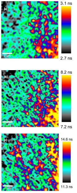
Figure 7. Spatially varying relaxation times at photon emission energies of 2.756eV (450nm), 2.611eV (475nm) and 2.480eV (500nm), respectively.
The reason for this difference is multi-layered. The difference of the indium concentration forms a potential landscape for electrons and holes. The diffusion of the carriers is restricted at large and flat potential valleys, thereby affecting the local relaxation time due to the flow of the surrounding carriers into this valley. A lateral quantum confinement is created along with the MQW at the potential valleys that are deep and tinier than about 10-50nm, where electrons and holes are trapped. This localization process dramatically improves the lifetime of the direct electron-hole-recombination.
Signal Propagation Through the Device
The starting point of the temporal decay of the emission also varies in space. For areas that have a larger distance to the bond pad of the back-side contact, the luminescence emission is delayed. This effect is shown as a contour plot in Figure 8. The corresponding time spectra are illustrated in Figure 9. The temporal and spatial distances of the red and yellow areas facilitate calculating a propagation speed of about 150km/s for the electrical pulse.
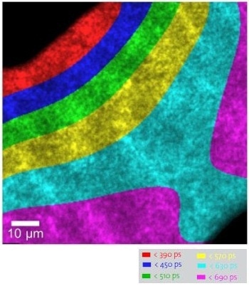
Figure 8. Temporal start of the luminescence emission.
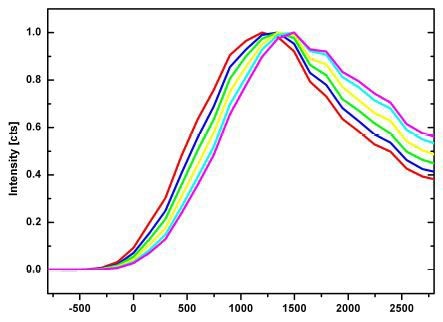
Figure 9. Average time spectra of the colored areas in Figure 8
Conclusion
The results clearly demonstrate the ability of the WITec microscope series equipped with a time correlated single photon counting module to perform time resolved photoluminescence studies of LEDs.

This information has been sourced, reviewed and adapted from materials provided by WITec GmbH.
For more information on this source, please visit WITec GmbH.