Temperature measurement is considered to be an extremely vital physical parameter when determining reliability, accuracy and quality of processes in industrial use as well as in almost every single human activity. Temperature sensors are developed with a variety of technologies to meet specific application needs.
IST AG has concentrated one part of the development and manufacturing on high-end thin-film temperature sensors. This knowledge is partially obtained from the semiconductor industry and enables the company to manufacture sensors with exceptional long-term stability, high accuracy, and high reliability and repeatability within a wide temperature range from -200 °C up to 1000 °C. The thin-film temperature sensors exhibit an extremely short response time due to low thermal mass and very small dimensions.
Temperature Sensors - Directly Welded Wires - Innovative Sensor Technology IST AG
It is an established fact that customers over time need a better long-term stability with increasing accuracy in a wider and wider temperature range. Due to the exceptional long-term stability of the IST AG thin film temperature sensors it is possible to guarantee the standard class B (DIN EN 60751; F 0,3), class A (DIN EN 60751; F 0,15) or class 1/3DIN EN 60751; F 0,1, and also to ensure even more precise accuracy classes such as 1/5 DIN or 1/10 DIN. IST AG manufactures and supplies a wide range of sensor elements in accuracies measured in class 1/5 DIN, 1/6 DIN or even 1/10DIN over a wide range of temperature.
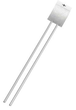
Figure 1. MiniSens temperature sensor (1 mm x 1.6 mm)
IST AG also offers customers a special nominal resistance at, for example, 0 °C or to measure the sensors in shifted tolerance bands such as (0 mK to 300 mK) at 0 °C instead of for example (-300 mk to +300 mK) at 0 °C to offeset a shift of Ohmic values during the assembly process by the customer.
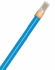
Figure 2. Temperature sensor with PTFE insulated wires
The behavior of the IST AG platinum temperature sensors is exactly described by the IST AG characteristic curve, which is based on over 20 years of measuring experience. With this knowledge, it is possible within a particular temperature range to measure individual sensor elements and extract individual polynomial values R(0), A and B from a polynomial of second order of type (R(T) = R0 (1 + A x T + B x T2)) in order to obtain the highest achievable accuracy.
Sensor elements are also offered in pairs with custom specific deviations (max.) and sensors are also offered in groups based on temperature coefficient and custom specific deviation (max.). Annually, IST AG produces more than 10 million sensors from a portfolio covering over 4000 different products.
The Process of CSPAB (Custom-Specific Product Approval Board)
Customer specific enquiries usually begin by taking contact to one of the IST AG sales specialists. The sales specialist discusses the specific application and requirements together with the customer. This is followed by discussing the project internally with relevant R&D engineers and submitting it to the CSPA board. The CSPA board consists of IST AG production and quality engineers, sales specialists, and developers contributing with specific product knowledge and expertise. The board evaluates the feasibility of the submitted solution and its product requirements to either approve or determine if further clarification is required. Samples are produced for customer validation only after the customer is satisfied with the proposed solution. When successful, IST AG will begin production and deliver the parts within a short time period.
More than 200 new sensor solutions, approved by the CSPA board, are manufactured each year, and these solutions are then added to the portfolio based on specific customer applications and requests.
As Easy as 1 – 2 – 3: Production of a Customized Temperature Sensor
Step 1
The production of a customized sensor begins by depositing a thin film metallic layer onto a ceramic substrate. This process is performed in IST AG’s modern clean rooms classified as ISO5 (meaning a maximum of 3520 particles per m3). During deposition, various possibilities of customization such as deposition material (Au, Cr, Ti, Ni or Pt) and substrate thicknesses (from 0.1 mm to 0.6 mm) are available.
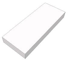
Figure 3. Ceramic substrate
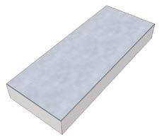
Figure 4. Ceramic substrate with-thin film metallic layer
Wet chemical cleaning processes and high temperature annealing steps are carried out after the deposition in order to ensure high quality and long term stable sensors.
Step 2
Multiple steps are involved to define the pattern of the sensor structure. The first step involves spin coating of a photo-sensitive resist onto the substrate. Next, the photo-sensitive resist is structured by exposition. Finally, the photo resist is removed leaving only the sensor structure on the chip.
During this step, it is essential to choose a specific mask. The final chip dimension, layout, and the resistive structure of the sensor element are determined by the mask. IST AG offers various standard chip dimensions with different resistive values and layouts based on specific customer requests. Resistive values between 50 Ω and 100,000 Ω and multiple resistances on one chip are also possible.
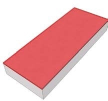
Figure 5. Substrate with photo-sensitive resist
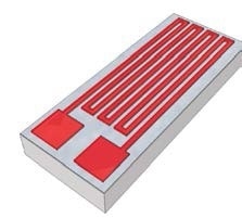
Figure 6. Substrate after exposition
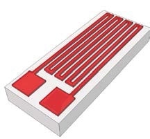
Figure 7. Photo-sensitive resist structured by exposition
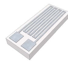
Figure 8. Structure after removal of photo-sensitive resist
Screen printing is then applied to the sensor pads in order to increase the strength between the wires and pads, considerably improving vibration and thermal cycling robustness. The resistive structure of each sensor element is separately laser-trimmed to attain the required resistive accuracy. An additional passivation layer is screen printed onto the element as a final process step in the clean room for further mechanical and chemical protection.
Figure 9. Sensor with passivation layer
Figure 10. Sensor with passivation layer and strengthend pads
Step 3
Contact with the element is essential to read the resistance values. For SMD and Flip-Chip sensor elements, HMP or LMP solder are directly deposited on contact pads instead of wires. Specific contact layers for bonding are also part of the IST AG portfolio. Different configurations are welded directly on the chip on automated welding machines for wired sensor elements. IST AG offers a wide range of wire material for example Ag, Au/Ni, Ag/Cu, Pt, Pt/Ni, Cu, Ni, Cu etc. configured as both single core and stranded wire. Insulation of the wires is required in many applications and IST AG can directly weld insulated wires on the sensor element. When direct welding is not an option, extension of the lead wires with laser welding or brazing is provided. The diameter and length of the wire can be customized as well as the design of the wire configuration, for example standard, perpendicular, or inverted welding. In addition, configurations with 3 or 4 wires in a variety of colors are also possible.
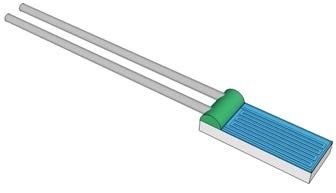
Figure 11. Sensor with welded wires and welding area covered with fixation paste to increase robustness
After welding, a fixation paste is applied on the contact area to increase robustness. Additionally, aging and thermal cycling the sensor elements are now ready for visual and electrical quality inspection prior to shipping.
A very sought after option is IST AG’s metalized back side feature. With this feature, customers can attain excellent thermal coupling by soldering directly to a metal surface or cap (Cu, titanium, stainless steel etc.). Additional options could be fitting of connectors onto wires, sensor elements inserted in round ceramic cases, injection molded housings, and sensor elements assembled in stainless steel probes.
Thanks to the excellent stability and accuracy, IST AG’s temperature sensors are used in all volumes – large and small – in industries such as satellite applications, process control over aerospace, medical and heating-ventilation. The IST AG sensors, whether it is a customized or standard solution, provide the optimal price to performance ratio with a short production time because of the excellent stability and accuracy of the sensors, competence of employees, and the flexibility in production.
Your Sensor is our Competence
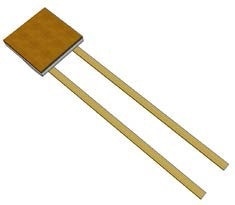
Figure 12. Temperature sensor with
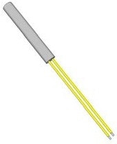
Figure 13. Sensor assembled in
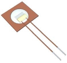
Figure 14. Sensor with metalized back side feature and soldering directly to a Cu surface
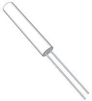
Figure 15. Sensor inserted in round ceramic case

This information has been sourced, reviewed and adapted from materials provided by Innovative Sensor Technology, USA Division.
For more information on this source, please visit Innovative Sensor Technology, USA Division.