Thanks to their high variety of properties, ceramic materials are used in an extensive range of application fields. Overall, ceramics are considered as materials with high-temperature resistivity and great mechanical properties. However, ceramic materials could also display for example, biological, optical or electrical properties. The properties of ceramics are greatly influenced by porosity, crystallography or chemical composition. Hence, they are used in many different areas ranging from disk brakes, bearings and grinding materials to coatings on biological implants or jet engine turbine blades.
Imaging Ceramics
Usually, ceramic materials are excellent electric and heat insulators; these properties make SEM imaging of ceramics more challenging. One of the methods for imaging non-coated insulating materials with reduced charging artifacts is using low electron beam energies. Increased surface sensitivity because of the small beam-interaction volume is an added benefit which results in higher spatial resolution. This in turn, makes surface features such as small pores, grain structure, nano-sized surface features or thin contamination surface layers more visible, see Figure 1 (right). However, with conventional scanning electron microscopes (SEM), it is difficult to image at low beam energies without affecting image quality and hence, more sophisticated electron optics and detection systems are required.

Figure 1. Ceramic samples with the E-T detector for topographic and material contrast. The ceramic sample on the left was imaged at 2 keV. The ceramic sample on the right was imaged at 500 eV for enhanced surface sensitivity.
TESCAN S8000 Microscope
These requirements are fulfilled by the new TESCAN S8000 microscope. It is fitted with the new BrightBeam™ SEM column technology whose objective is a combination of Wide Field Optics™ and electrostatic-magnetic lenses. The BrightBeam™ column realizes field-free ultra-high resolution (UHR) through a beam guiding potential which shifts the energy of the primary beam while the electrostatic part of the lens decelerates and focuses the beam and also aids in enhancing signal collection by driving electrons into the column. This minimizes aberrations as the beam is focused at higher energies.
The design of the lens enhances resolution particularly at low beam energies making the TESCAN S8000 microscope an ideal instrument for resolving nanostructures and examining delicate samples thus useful for nanocharacterization of ceramics. The column is equipped with a powerful detection system comprised of in-beam detectors with angle-selective and energy-filtering capabilities, and the E-T in-chamber detector. The design of the electron column ensures high signal throughput even at ultra-low (e.g. 500 eV) beam energies – a regime in which the small beam spot size enables resolving nano-sized features, see Figure 1.
In addition, the TESCAN S8000 microscope comes with the Multi-detector – a powerful and versatile detector that features a filtering grid, a conversion surface, and a biased scintillator which allows energy-filtered collection of narrow-angle electrons.
The filter grid can be set at a defined bias potential to filter out certain electron signals and collect only electrons within a defined range energy window, the width of which, can be tuned to explore different types of contrast (see Figure 2) from pure topographic (only SE signal) to material (only BSE) or, an extremely narrow energy window for ultimate surface sensitivity and low-loss BSE imaging. It is also possible to use the energy-filtering capability for minimizing charging artifacts during imaging as only a portion of a selected energy spectrum is filtered out.
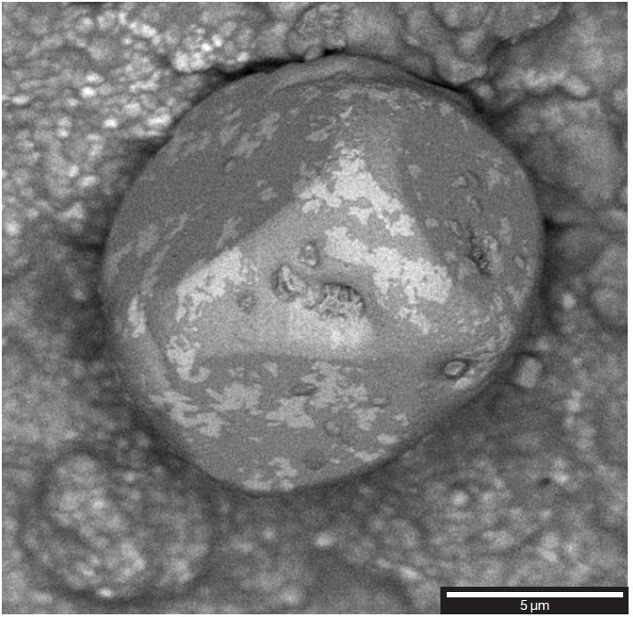
Figure 2. Ceramic sample imaged at 500 eV with the Multidetector, where the energy-filtering grid has been set to detect only the BSE signal.
TESCAN Group
Founded in 1991 by a group of managers and engineers from Tesla with its electron microscopy history starting in the 1950’s, today TESCAN is a globally renowned supplier of Focused Ion Beam workstations, Scanning Electron Microscopes and Optical Microscopes. TESCAN’s innovative solutions and collaborative nature with its customers have won it a leading position in the world of nano- and microtechnology. The company is proud to participate in premier research projects with prominent institutions across a range of scientific fields. TESCAN provides its clients with leading-class products in terms of value, quality and reliability. TESCAN Group is the North American arm of TESCAN Group, a multinational company established by the merger of Czech company TESCAN, a leading global supplier of SEMs and Focused Ion Beam workstations, and the French company ORSAY PHYSICS, a world leader in customized Focused Ion Beam and Electron Beam technology.

This information has been sourced, reviewed and adapted from materials provided by TESCAN Group.
For more information on this source, please visit TESCAN Group.