In semiconductor technologies, one of the most crucial techniques is to control the electrical properties of semiconductors by doping them with impurity. This technique could enable the conversion of carrier type from p-type to n-type carriers, thereby forming a pn homojunction.
Image Credit: Macro photo/Shutterstock.com
In the case of nominally undoped semiconductors, the carrier type is often governed by the defects with a low ionization energy and low formation enthalpy. This generally renders carrier-type conversion challenging.
Tin monosulfide (SnS) is a potential material for developing a solar light absorber for thin-film solar cells. It is made of non-toxic and abundant elements and shows a suitable optical property for solar cells. In general, SnS shows p-type conduction because of the intrinsic defects. The acceptor-type Sn vacancy (VSn) easily forms under S-rich conditions.
When it comes to SnS bulk pellets and single crystals, it was identified that substitutional anion doping with S2– that has halide ions (such as Cl– and Br–) enabled successful n-type electrical conduction. This doping technique is more propitious for practical use compared to the solid solutions between PbS and SnS (Sn1−xPbxS), where x > 0.2.
It has been proposed that acceptor-type defects such as VSn and SnS and ambipolar defects such as VS—both of which are caused by sulfur deficiencies—compensate the electrons added by halogen doping. This prevents the halogen-doped SnS thin films from showing n-type conduction. Hence, novel thin film deposition methods are required to overcome this issue.
In a study published in Physical Review Materials, the combination of radiofrequency (RF) magnetron sputtering and an RF sulfur plasma source was used to fabricate n-type SnS thin films. The use of the sulfur plasma source for deposition was found to considerably inhibit the formation of acceptor-type defects in the SnS films, possibly VSn and SnS, as well as ambipolar VS.
This is crucial in achieving n-type conduction in Cl-doped SnS thin films. The fabrication method shown here for n-type SnS thin films is predicted to transform SnS solar cells—from heterojunctions created in the past 20 years to homojunctions that exhibit considerably higher efficiency.
Methodology
Fabrication of SnS thin films was achieved using RF-magnetron sputtering. The dependence of the physical properties of SnS thin films on the substrate temperature was analyzed by using a SiO2 glass substrate measuring 50 × 50 mm with a temperature gradient of 221 °C–341 °C across it. The deposition time was set as 30 minutes. The sputtering target used in the experiment was a piece of undoped SnS with a diameter of 2 inches.
Chlorine (Cl) was supplied to the deposition vacuum chamber before performing thin film deposition. This was done by exposing a Cl-containing SnS target to Ar plasma under conditions identical to that of thin-film deposition for 30 minutes. Here, a temporary substrate was placed on the substrate holder.
The deposition chamber was then evacuated to its base pressure of less than 5 × 10⁻⁴ Pa. Subsequently, the substrate was replaced. Sulfur deficiency in the resulting thin films was prevented by using a sulfur plasma source together with RF sputtering.
Results
Figure 1(a) shows that all x-ray diffraction (XRD) peaks of the resulting films are indexed as α-SnS. Moreover, there were no impurity phases such as polymorphs of SnS, SnS2, and Sn2S3 regardless of whether the sulfur plasma was supplied during deposition.
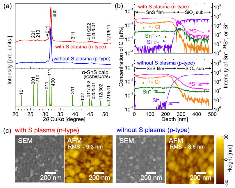
Figure 1. Structural, compositional, and morphological analysis of Cl-doped SnS thin films deposited with and without a sulfur plasma supply. (a) X-ray diffraction (XRD) profiles of films deposited at Tsub = 333 °C, together with a reference pattern of α-SnS (ICSD#24376). (b) Depth profile of Cl concentration and normalized intensities of secondary ions of Sn−, 34S−, and Si− in the films deposited at Tsub = 333 °C. (c) Scanning electron microscopy (SEM) and atomic force microscopy (AFM) images of the surface of SnS thin films deposited at Tsub = 333 °C. The root-mean-square (RMS) roughness is also shown. Image Credit: Suzuki, et al., 2021
As shown in Table 1, the chemical compositions of the films that were deposited in the presence and absence of sulfur plasma supply were assessed by x-ray fluorescence spectroscopy (XRF).
Table 1. Physical properties of SnS thin films prepared at Tsub = 333 °C with and without a sulfur plasma supply. All results were obtained at room temperature, except that the Seebeck coefficients were measured at 25 °C–50 °C. Source: Suzuki, et al., 2021
| |
SnS thin films deposited |
| |
With sulfur plasma |
Without sulfur plasma |
| Thickness (nm) |
250 |
190 |
| Atomic ratio, S/(Sn + S) |
0.507 |
0.498 |
| Cl concentration (cm–3) |
3.7 × 10¹⁸ |
4.6 × 10¹⁸ |
| Hall coefficient (cm3 C–1) |
–2.6 × 100 |
+4.8 × 10³ |
| Seebeck coefficient (μVK–1) |
–6.3 × 101 |
+1.4 × 10⁴ |
| Carrier type |
n-type |
p-type |
| Electrical conductivity (S cm–1) |
9.2 × 10⁻² |
3.1 × 10⁻⁴ |
| Carrier concentration (cm–3) |
2.4 × 10¹⁸ |
1.4 × 10¹⁵ |
| Hall mobility (cm2 V–1 s–1) |
2.4 × 10⁻¹ |
1.5 × 100 |
The depth profile of Cl concentration as well as the intensities of the secondary ions of Sn–, Si–, and 34S– governed by time-of-flight secondary ion mass spectroscopy are illustrated in Figure 1(b).
The atomic force microscopy (AFM) and surface scanning electron microscopy (SEM) observations shown in Figure 1(c) demonstrate that the resulting SnS films are made of nearly circular grains with a 10–200 nm diameter whether or not there was sulfur plasma supply. By contrast, grain size tends was found to be somewhat smaller (<100 nm) in the film deposited in the presence of sulfur plasma supply.
From Figure 2(a), it is evident that the binding energies of the valence band edge, S 2p, and Sn 3d peaks of the film (the n-type film) deposited in the presence of sulfur plasma supply shifted downward by ∼0.3 eV than the film (p-type) deposited in the absence of sulfur plasma. From these findings, it is clear that the carrier type of the thin films is governed by the presence or absence of sulfur plasma supply.
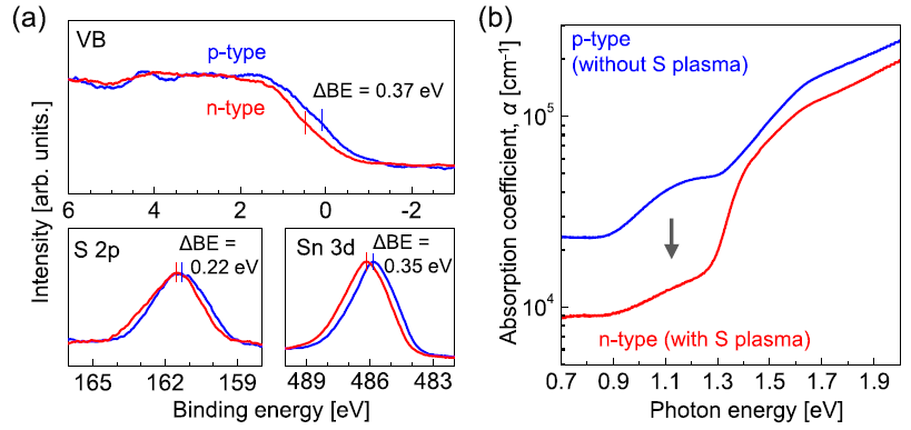
Figure 2. (a) X-ray photoelectron spectroscopy (XPS) spectra (excitation source: Ag Lα) of SnS films deposited at Tsub = 222 °C for the valence band (VB), S 2p, and Sn 3d core levels. Differences in the binding energies between n- and p-type films (ΔBE) are shown in each plot. A total resolution of ∼0.5 eV for the measurement resulted in significant spectral broadening. The displayed spectra were obtained by the moving average of the original results. Other characteristics of this film (Tsub = 222 °C) are discussed in the last half of main text. (b) Absorption spectra of the n- and p-type SnS thin films prepared at Tsub = 333 °C. The broad peak centered at 1.1 eV is significant only for the p-type film. Image Credit: Suzuki, et al., 2021
From Figure 2(b), it can be observed that besides the steep slope from 1.3 eV corresponding to the basic SnS absorption, a broad absorption at ∼1.1 eV was considerably more obvious in the film (p-type film) deposited in the absence of sulfur plasma supply than the film (n-type film) deposited in its presence.
Figure 3(a) is a plot of the temperature-dependent carrier concentration in both the p-type and n-type films.
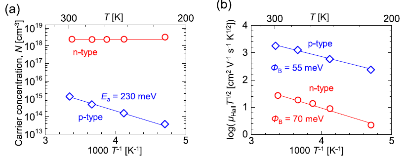
Figure 3. (a) Temperature dependence of carrier concentration and (b) μHallT1/2 of SnS thin films deposited at Tsub = 333 °C. The activation energy (Ea) and grain boundary potential barriers (ΦB) were estimated according to the following formulas: N = N0exp(–Ea/kT), where N0 is a prefactor and k is the Boltzmann constant, and μHall = Le(1/2πm*kT )1/2exp(–ΦB/kT), where L is the grain size, e is elementary charge, and m* is the effective mass. The solid lines were added to guide the eye. Image Credit: Suzuki, et al., 2021
The temperature dependence of the Hall mobility for both films is illustrated in Figure 3(b). For both n-type and p-type SnS thin films, the Hall mobility decreases with a decrease in temperature. This corresponds to the fact that phonon scattering or ionized scattering in these films do not govern carrier transport.
Figure 4(a) shows that there was a shift in the primary peaks corresponding to 400 diffractions toward a lower diffraction angle with a decrease in the substrate temperature. This shows that there was an increase in the lattice constant in the a-axis (a0) with a decrease in the substrate temperature.
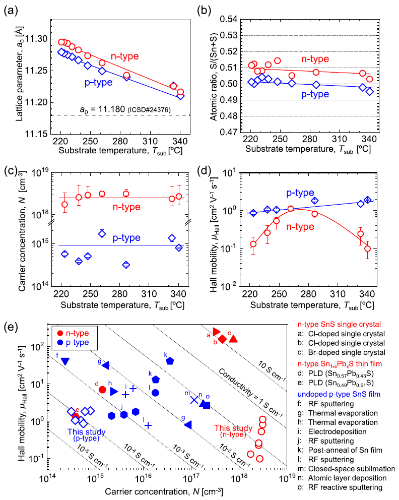
Figure 4. Substrate temperature dependence of the various properties of the obtained SnS thin films. (a) Lattice parameter of a0 of the obtained thin films determined by 400 diffraction peaks (for the x-ray diffraction (XRD) profiles. (b) Chemical composition determined by x-ray fluorescence spectroscopy (XRF). (c) Carrier concentration and (d) Hall mobility of SnS thin films measured at room temperature. All solid lines in the figures were added to guide the eye. (e) Comparison of electrical properties of n- and p-type SnS thin films obtained in this paper and those of previously reported n- and p-type SnS, and n-type Sn1−xPbxS solid solutions. Image Credit: Suzuki, et al., 2021
A plot between the chemical composition of SnS thin films and the substrate temperature is shown in Figure 4(b). Figures 4(c) and 4(d) illustrate the dependence of the electrical properties on the substrate temperature for both n-type and p-type SnS thin films. The n-type SnS thin films fabricated in this study exhibit a low Hall mobility and high carrier concentration that the p-type films and n-type bulk single crystals reported earlier (see Figure 4(e)).
The use of sulfur plasma supply during deposition is advantageous for fabricating high-quality undoped p-type SnS thin films as it effectively inhibits the formation of acceptor-type defects.
The sulfur plasma can be supplied to fabricate high-quality thin films with both n-type and p-type conduction. This technique will certainly be crucial for achieving highly efficient SnS homojunction solar cells.
Conclusion
This study achieved n-type electrical conduction in SnS thin films through sulfur plasma supply at the time of deposition in conjunction with Cl doping. In the absence of sulfur plasma supply, the fabricated SnS thin films showed p-type conduction despite having a comparable amount of Cl donors.
The fabrication technique discussed in this study can be used for an extensive range of sputtering conditions. This is because n-type conduction was achieved irrespective of the substrate temperature. To date, SnS heterojunction solar cells have exhibited a stagnant conversion efficiency at low values (4%–5%).
New techniques to produce n-type SnS thin films will allow the fabrication of SnS pn homojunctions and transform the SnS solar cell technology to a shift from heterojunctions to homojunctions to achieve high conversion efficiency.
Journal Reference:
Suzuki, I., Kawanishi, S., Bauers, S. R., Zakutayev, A., Lin, Z., Tsukuda, S., Shibata, H., Kim, M., Yanagi, H., Omata, T. (2021) n-type electrical conduction in SnS thin films. Physical Review Materials, 5, p. 125405. Available online: https://journals.aps.org/prmaterials/pdf/10.1103/PhysRevMaterials.5.125405.
References and Further Reading
- Amano, H., et al. (1989) p-type conduction in Mg-doped GaN treated with low-energy electron beam irradiation (LEEBI). Japanese Journal of Applied Physics, 28, L2112. doi.org/10.1143/JJAP.28.L2112.
- Vidal, J., et al. (2012) Band-structure, optical properties, and defect physics of the photovoltaic semiconductor SnS. Applied Physics Letters, 100, p. 032104. doi.org/10.1063/1.3675880.
- Xiao, Z., et al. (2018) Multiple states and roles of hydrogen in ptype SnS semiconductors. Physical Chemistry Chemical Physics, 20, p. 20952. doi.org/10.1039/C8CP02261E.
- Malone, B. D., et al. (2014) First principles study of point defects in SnS. Physical Chemistry Chemical Physics, 16, p. 26176. doi.org/10.1039/D1CP04567A.
- Sinsermsuksakul, P., et al. (2012) Antimony-Doped Tin (II) Sulfide Thin Films. Chemistry of Materials, 24, p. 4556. doi.org/10.1021/cm3024988.
- Dussan, A., et al. (2010) Effect of substitution of Sn for Bi on structural and electrical transport properties of SnS thin films. Journal of Materials Science, 45, pp. 2403–2407. doi.org/10.1007/s10853-010-4207-z.
- Yanagi, H., et al. (2016) Hosono, n-type conduction in SnS by anion substitution with Cl. Applied Physics Express, 9, p. 051201. doi.org/10.7567/APEX.9.051201.
- Iguchi, Y., et al. (2018) Single-crystal growth of Cl-doped n-type SnS using SnCl2 self-flux. Inorganic Chemistry, 57(12), pp. 6769–6772. doi.org/10.1021/acs.inorgchem.8b00646.
- Kawanishi, S., et al. (2020) Growth of large single crystals of n-type SnS from halogen-added Sn flux. Crystal Growth & Design, 20, p. 5931. doi.org/10.1021/acs.cgd.0c00617.
- Hu, X., et al. (2019) Thermoelectric transport properties of n-type tin sulfide. Scripta Materialia, 170, p. 99 doi.org/10.1016/j.scriptamat.2019.05.043.
- Iguchi, Y., et al. (2018) Segregation of chlorine in n-type tin monosulfide ceramics: actual chlorine concentration for carrier-type conversion. Applied Physics Letters, 112, 202102. doi.org/10.1063/1.5027679.
- Xiao, Z., et al. (2015) Route to n-type doping in SnS. Applied Physics Letters, 106, p. 152103. doi.org/10.1063/1.4918294.
- Ran, F.-Y., et al. (2015) Kamiya, n-type conversion of SnS by isovalent ion substitution: geometrical doping as a new doping route. Scientific Reports, 5, p. 10428. doi.org/10.1038/srep10428.
- Honig, R E & Kramer, D A (1969) Vapor pressure data for the solid and liquid elements, RCA Review, 30, p. 285.
- Subramaniyan, A., et al. (2014) Non-equilibrium deposition of phase pure Cu2O thin films at reduced growth temperature. APL Materials, 2, p. 022105. doi.org/10.1063/1.4865457.
- See Supplemental Material at https://www.aps.org/ 10.1103/PhysRevMaterials.5.125405 for detailed information on thin film fabrication and characterization, temperature gradient in the substrate, crystal structure, EBSD mapping, in-plane analysis by TOF-SIMS measurement, additional SEM and AFM images of thin film morphology, XPS with Ag-Lα excitation, optical properties and determination of band gaps, double log plots of Hall mobility vs temperature, detailed dependence of electrical properties on substrate temperature, and XRD profiles of SnS thin films deposited at various substrate temperatures and thickness of thin films, which includes Ref.
- Baranowski, L. L., et al. (2014) Control of Doping in Cu2SnS3 through Defects and Alloying. Chemistry of Materials, 26(17), pp. 4951–4959. doi.org/10.1021/cm501339v.
- Arepalli, V. K., et al. (2018) Influence of working pressure on the structural, optical, and electrical properties of RF-sputtered SnS thin films. Superlattices and Microstructures. 122, p. 253. doi.org/10.1016/j.spmi.2018.08.001.
- Baby, B H & Mohan, D B (2019) The effect of in-situ and post deposition annealing towards the structural optimization studies of RF sputtered SnS and Sn2S3 thin films for solar cell application. Solar Energy, 189, p. 207. doi.org/10.1016/j.solener.2019.07.059.
- Tauc, J., et al. (1966) Optical Properties and Electronic Structure of Amorphous Germanium. Physica Status Solidi, 15, p. 627. doi.org/10.1002/pssb.19660150224.
- Yanuar, et al. (2000) SnS thin films grown by close-spaced vapor transport. Journal of Materials Science Letters, 19(23), pp. 2135–2137. doi.org/10.1023/A:1026778810656.
- Ran, F.-Y., et al. (2016) SnS thin films prepared by H2S-free process and its p-type thin film transistor. AIP Advances, 6, p. 015112. doi.org/10.1063/1.4940931.
- Devika, M., et al. (2021) Reddy, Influence of annealing on physical properties of evaporated SnS films. Semiconductor Science and Technology, 21, 115. doi.org/10.1088/0268-1242/21/8/025.
- . Park, H. H., et al. (2015) Co-optimization of SnS absorber and Zn(O,S) buffer materials for improved solar cells. Progress in Photovoltaics Research Applications, 23, p. 901. doi.org/10.1002/pip.2504.
- Noguchi, H., et al. (1994) Characterization of vacuum-evaporated tin sulfide film for solar cell materials. Solar Energy Materials and Solar Cells, 35, p. 325. doi.org/10.1016/0927-0248(94)90158-9.
- Sánchez-Juárez, A., et al. (2005) Fabrication of SnS2/SnS heterojunction thin film diodes by plasma-enhanced chemical vapor deposition. Thin Solid Films, 480–481, pp. 452–456. doi.org/10.1016/j.tsf.2004.11.012.
- Seto, J. Y. W., et al. (1975) The electrical properties of polycrystalline silicon films. Journal of Applied Physics, 46, p. 5247. doi.org/10.1063/1.321593.
- Ran, F.-Y., et al. (2014) Growth of high-quality SnS epitaxial films by H2S flow pulsed laser deposition. Applied Physics Letters, 104, p. 072106. doi.org/10.1063/1.4866009.
- Zhou, B., et al. (2017) Thermoelectric properties of SnS with Na-doping. ACS Applied Materials Interfaces, 9, p. 34033. doi.org/10.1021/acsami.7b08770.
- . Hegde, S. S., et al. (2018) Vacuum annealed tin sulfide (SnS) thin films for solar cell applications. Surface Interfaces, 10, p. 78. doi.org/10.1016/j.surfin.2017.12.003.
- Kawano, Y., et al. (2015) Impact of growth temperature on the properties of SnS film prepared by thermal evaporation and its photovoltaic performance. Current Applied Physics. doi.org/10.1016/j.cap.2015.03.026.
- Ginley, D S (Ed.) (2011) Handbook of Transparent Conductors. Springer: US, Boston.
- Reddy, K. T. R., et al. (2006) Photovoltaic properties of SnS based solar cells. Solar Energy Materials and Solar Cells, 90(18–19), pp. 3041–3046. doi.org/10.1016/j.solmat.2006.06.012.
- Schneikart, A., et al. (2013) Efficiency limitations of thermally evaporated thin-film SnS solar cells. Journal of Physics D: Applied Physics, 46, p. 305109. doi.org/10.1088/0022-3727/46/30/305109.
- Sugiyama, M., et al. (2021) Band offset of SnS solar cell structure measured by X-ray photoelectron spectroscopy. Thin Solid Films, 519(21), pp. 7429–7431. doi.org/10.1016/j.tsf.2010.12.133.
- . Sinsermsuksakul, P., et al. (2013) Enhancing the efficiency of SnS solar cells via band-offset engineering with a zinc oxysulfide buffer layer. Applied Physics Letters, 102, p. 053901. doi.org/10.1063/1.4789855.
- Sinsermsuksakul, P., et al. (2014) Overcoming efficiency limitations of SnS-based solar cells. Advanced Energy Materials, 4, p. 1400496. doi.org/10.1002/aenm.201400496.
- Sun, L., et al. (2013) Band alignment of SnS/Zn(O,S) heterojunctions in SnS thin film solar cells. Applied Physics Letters, 103, p. 181904. doi.org/10.1063/1.4821433.
- Yun, H., et al. (2019) Efficient nanostructured TiO2/SnS heterojunction solar cells. Advanced Energy Materials, 9, 1901343. doi.org/10.1002/aenm.201901343.
- Lin, X., et al. (2016) Numerical analysis of SnS homojunction solar cell. Superlattices and Microstructures, 91, p. 375. doi.org/10.1016/j.spmi.2016.01.037.
- Kawanishi, S., et al. (2021) Omata, SnS homojunction solar cell with ntype single crystal and p-type thin film. Solar RRL, 5, p. 2000708. doi.org/10.1002/solr.202000708.
- Ghosh, B., et al. (2011) Structural and optoelectronic properties of vacuum evaporated SnS thin films annealed in argon ambient. Applied Surface Science, 257, p. 3670. doi.org/10.1016/j.apsusc.2010.11.103.
- Huang, W., et al. (2012) Electrical and optical properties of In-doped SnS thin films prepared by thermal evaporation. ECS Transactions, 44 (1), pp. 1295–1301. doi.org/10.1149/1.3694463.
- Liu, Y., et al. (2019) Electrodeposition of copper-doped SnS thin films and their electric transmission properties control for thermoelectric enhancement. Journal of Materials Science: Materials in Electronics, 30(23). doi.org/10.1007/s10854-019-01924-7.
- Minnam Reddy, V. R., et al. (2015) Development of sulphurized SnS thin film solar cells Current Applied Physics, 15(5), pp. 588–598. doi.org/10.1016/j.cap.2015.01.022.
- Jang, B., et al. (2017) Fabrication of single-phase SnS film by H2 annealing of amorphous SnSx prepared by atomic layer deposition. Journal of Vacuum Science & Technology A, 35, p. 031506. doi.org/10.1116/1.4978892.
- Zhao, L., et al. (2016) In situ growth of SnS absorbing layer by reactive sputtering for thin film solar cells. RSC Advances, 6, p. 4108. doi.org/10.1039/C5RA24144H.
- Kraut, E. A., et al. (1980) Precise Determination of the Valence-Band Edge in X-Ray Photoemission Spectra: Application to Measurement of Semiconductor Interface Potentials. Physics Review Letters, 44, p. 1620. doi.org/10.1103/PhysRevLett.44.1620.