Thin films continue to draw the focus of researchers. This article takes a current and closer look at their applications, variable deposition methods, and future uses.
What Do We Know About Thin Films?
‘Thin Film’ is a relative term that expresses the much lesser thickness of a two-dimensional (2D) material compared to its substrate/s, whether its purpose is to cover the substrate or to be sandwiched in between two surfaces. In modern industrial applications, the thickness of these thin films usually ranges from sub-nanometer (nm) atomic level size (i.e., < 1 nm) to several micrometers (µm). Single-layer graphene has a thickness of one carbon atom (i.e., ~ 0.335 nm).
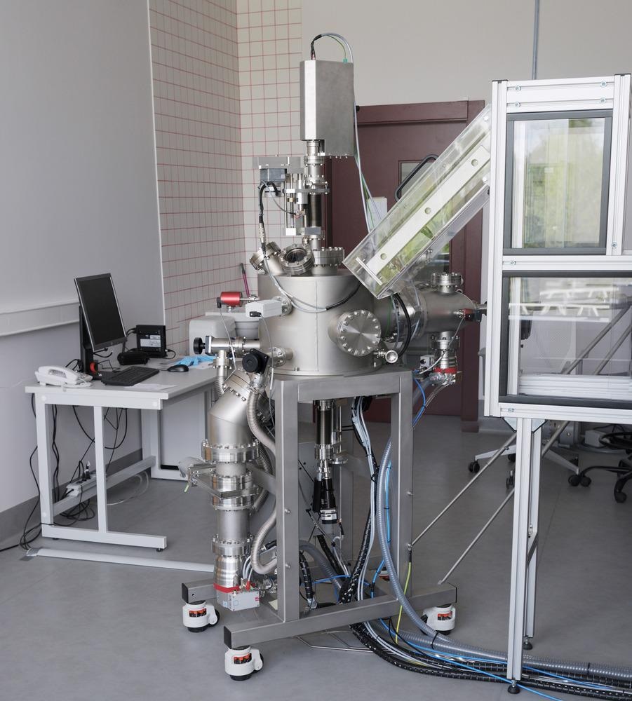
Pulsed laser deposition system for thin film growth. Image Credit: Tomas Salkus/Shutterstock.com
Applications of Thin Films
The oldest applications of thin films were for decoration and painting purposes during prehistoric periods. Nowadays, a thin film of precious metals such as bronze, silver, gold, and platinum is coated on luxurious items and ornaments.
The most common application of thin films is to physically protect a surface from wear, impacts, scratches, erosions, and abrasions. Dimond-like carbon (DLC) and MoSi2 layers are used to protect car engines against abrasion and high-temperature corrosion, which is caused due to friction between mechanically moving parts.
Alumina (Al2O3) has a Mohs hardness of 9.0, which is used to protect sensitive metal surfaces against erosion and corrosion, and for thermal insulation. SiO2 and SiC also find their applications in protecting pipes and stainless steel components. TiN and TiC thin films are used in microelectronic chips to separate aluminum conductors from silica (SiO2) insulators so that the formation of Al2O3 can be suppressed.
More from AZoM - Polyether Ether Ketone: Latest Developments and Applications
Thin films are also used to protect chemically reactive surfaces from their surrounding environment, whether it is oxidation or hydration due to moisture. In the field of semiconductor devices, dielectric thin film separators, thin-film electrodes, and electromagnetic interference (EMI), shielding conducting thin films have garnered a lot of attention. In particular, metal-oxide-semiconductor field-effect transistors (MOSFETs) incorporate chemically and thermally stable dielectric thin films such as SiO2, whereas complementary metal-oxide-semiconductors (CMOS) incorporate conducting Cu thin films.
Thin-film electrodes have increased the energy density to volume ratio of supercapacitors by multi-folds. Moreover, metal thin films, and currently MXenes (transition metal carbides, nitrides, or carbonitrides) perovskite ceramic thin films are being extensively used for EMI shielding of electronic components.
BiFeO3, PbZrTi3, and amorphous Si thin films have made their place in non-volatile memory devices owing to their excellent magnetic properties. Additionally, cesium lead halides, copper indium gallium selenide, and CdTe thin films have shown promising characteristics in the photovoltaic (PV) sector.
Thin Films Deposition Methods
Physical Vapor Deposition (PVD)
In PVD, the targeted material is evaporated and transferred into a vacuum chamber containing the substrate. The vapor starts to deposit on the substrate surface due to condensation alone. The vacuum prevents the mixing of impurities and collisions between vapor molecules and residual gas molecules.
The turbulence in the inducted vapor, the temperature gradient, the vapor flow rate, and the latent heat of the targeted material play a significant role in determining the uniformity and processing time of the thin film. The evaporation techniques include resistance heating, electron beam heating, and most recently molecular-beam epitaxy.
The drawbacks of conventional PVD are its incapability to evaporate materials that have a very high melting point and the structural changes induced in the deposited material due to the evaporation-condensation process. Magnetron sputtering is a new generation of physical deposition methods that resolves these issues. In magnetron sputtering, the molecules of the target material are ejected out (sputtered) due to the bombardment of high-energy positive ions passing through a magnetic field produced by a magnetron.
Physical Vapour Deposition sputtering process (PVD)
Video Credit: Plansee High Performance Materials/Youtube.com
Chemical Vapor Deposition (CVD)
CVD is similar to PVD in terms of the use of evaporation of the target material. However, the deposition mechanism is chemically driven rather than by pure condensation. Either multiple target materials are made to chemically react in the vapor phase inside the chamber and the resulting products get deposited on the neutral substrate, or the substrate itself is made to chemically react with the vapor to form a thin film at the interface.
The surface roughness and the stability of the hydrodynamic and thermal boundary layer play role in CVD. A variation of CVD, plasma-enhanced CVD (PECVD), is currently used, in which plasma energy is used along with thermal energy to enhance the dissociative reaction between reacting vapors. Similarly, volatile metalorganic precursors are used in metalorganic CVD (MOCVD) instead of inorganic compounds.
Thin Film Properties
The thin films deposited through evaporation can have a polycrystalline, amorphous, or epitaxial columnar grain structure based on the substrate temperature, pressure, deposition rate, and alignment of vapor molecules with the substrate. The deposition rate and deposition temperature, particularly, affect the target atom diffusion on the already formed layer. Moreover, the internal stresses developed during the deposition determine the mechanical strength of the fabricated film.
Furthermore, the electron mean free path of the thin films is higher than that of bulk materials owing to reduced electron scattering. Moreover, the high interfacial energy of thin films increases their adhesion to the substrate surface.
Conclusions
Thin films have earned a special place in modern electronic, optical, mechanical, photonic, thermal, and magnetic devices, and even decorating items owing to their versatility, compactness, and functionalizing properties. PVD and CVD are the most commonly used evaporative vapor deposition techniques to achieve thin films of thickness ranging from a few nm to several micrometers.
The final morphology of the deposited film affects their performance and effectiveness. Nevertheless, the thin film evaporation deposition techniques need further research for the accurate prediction of film properties from available input process parameters, selected target material, and substrate properties.
References and Further Reading
Jameel, Dler. (2015). Thin Film Deposition Processes. International Journal of Modern Physics and Applications. 1. 193-199 https://www.researchgate.net/publication/281090098_Thin_Film_Deposition_Processes
Acosta, E. (2021, October 20). Chapter: Thin Films/Properties and Applications. InTechOpen. https://www.intechopen.com/chapters/75002
https://www.ndsu.edu/pubweb/~qifzhang/Tech_Sputter-01.pdf
Goeke, R. S. (2014, May 1). Thin Films Deposition Methods Tutorial. OSTI. https://www.osti.gov/biblio/1145751
Disclaimer: The views expressed here are those of the author expressed in their private capacity and do not necessarily represent the views of AZoM.com Limited T/A AZoNetwork the owner and operator of this website. This disclaimer forms part of the Terms and conditions of use of this website.