Serving as the interface between the semiconductor chip and its macro-environment, semiconductor/integrated circuit (IC) packaging plays a significant function in the electronic industry. For a semiconductor to function successfully over many years of use, each chip must be shielded from the elements and potential stresses.
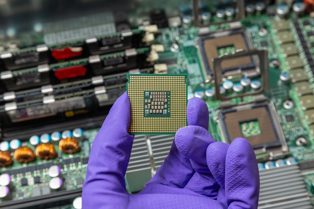
Image Credit: Stas Knop/Shutterstock.com
A Brief Introduction to Semiconductor/IC Packaging
IC packaging is a technique for shielding semiconductor equipment from ambient physical damage or degradation by wrapping them in ceramics or polymer packaging materials. There are several varieties of integrated circuits, each with its own circuit design and outer shell requirements. This leads to many sorts of IC package designs and classification schemes. With the evolution of technology, there is a growing desire for effective yet lightweight electronics, which is pushing the development of innovative packaging strategies.
Significance of Semiconductor Packaging
Since the 1970s, when producers of electronic packaging began employing ball grid array (BGA) containers, semiconductor packaging has evolved. Semiconductor components are generally fragile and lack the connections or pins necessary for attachment to a circuit board. Chip carriers will be employed to safeguard the fragile layout of integrated circuits and offer pin connections as a result of the introduction of semiconductor packaging.
In addition, the packages are composed of specific components that enhance the overall efficiency of the semiconductor technology and assure its dependability. Typically, the leads are composed of copper with a thin tin coating, with finer wires connecting the package. They help make a robust junction between the terminals and the electronic circuit. After this, the leads are attached to the conducting pads on the semiconductor die and then soldered to the PCB on the packages outside.
There are several varieties of semiconductor packages, each with a unique purpose.
DIP Semiconductor Packaging (DIP)
DIP stands for “Dual In-line Package.” This form of through-hole mount package has protruding lead pins on both sides of the package. Even though the standard pin pitch is 2.54mm (100mils), there is additionally 1.778mm (70mils) packages utilized in the semiconductor industry.
Dual in-line package (DIP) is one of the oldest forms of semiconductor packaging, and it remains popular in the industry. The pins are organized in a grid and are compatible with printed circuit boards (PCB). The DIP is composed of ceramic or plastic components. One of the benefits of DIP is that it is economical and simple to manufacture. But, DIP's size and pin count constraints render it unsuitable for newer high-density integrated circuits (ICs).
Quad Flap Package (QFP)
It is a surface mount package type. Lead pins protrude from each of the four edges of a QFP package. This particular packing style is distinguished by its leads' gull-wing (L-shaped) arrangement. There are several possible pin pitches, including 1.0mm, 0.8mm, 0.65mm, 0.5mm, 0.4mm, and 0.3mm.
The smaller, more flexible gull-wing leads improve secondary dependability (package-to-PCB reliability). Each of the four sides is L-shaped. Finely etched or stamped lead frames enable QFPs to accommodate more leads and have a smaller profile, resulting in improved electrical properties and shorter interconnects.
The QFP's pins are minute and closely spaced. Mishandling may easily cause damage and distortion. Also, it is quite difficult to alter them appropriately. They must be handled with care to prevent damage and are typically shipped in "waffle" packaging for adequate protection. Due to the large number of pins that QFPs may support, printed circuit boards must be designed with special care. High pin counts might make track density problematic around the device.
The QFP is composed of plastic components, rendering it lightweight and economical. The QFP offers several benefits, including compact size, a high pin count, and excellent thermal performance. Yet, its low thermal dissipation capabilities might compromise the ICs' dependability.
System-In-Package (SIP)
A system in package, or SiP, is a method of integrating many ICs into a single package. It is a form of a through-hole mount package that has protruding lead pins on one side. When mounted on a printed circuit board, the component stands upright. Instead of placing chips on a printed circuit board, they can be consolidated into a single package to save money or reduce the distance that electrical impulses must travel.
Silicon dies comprising distinct circuits based on different process nodes can be mounted vertically or horizontally on a SIP substrate. The package has intrinsic wiring that joins all the dies into a working system. System-in-package methods often employ wire bonding or bumping technologies.
The SIP technique enables semiconductor manufacturers to engage with more abstract building blocks, providing them with the benefits of greater turnover rates and a shorter design cycle overall. Several wireless applications (Bluetooth, WiFi) require an antenna. In SIP packaging, an antenna may be inserted at a very short distance from the RF IC, resulting in enhanced wireless solution performance.
Grid Array Packaging
A package containing leads organized in a grid pattern on one side. There are two varieties: PGA types with through-hole mounting and BGA types with surface mounting.
A Pin Grid Array (PGA) is a form of packaging with through-hole mounting. It is a nailbrush-shaped container with arranged lead pins positioned vertically on the bottom of the package. The pin pitch is 2.54 millimeters. It typically contains 64 to 447 pins. To cut costs, there are plastic PGAs that may be employed as the basic substrate of the package rather than glass epoxy resin printed circuit boards.
Ball Grid Array (BGA) is a form of surface-mount packaging that makes the electrical connection between the IC and the PCB using a grid of solder balls. On the backside of the BGA package is a network of solder balls arranged in a square or rectangular form. The BGA is composed of ceramic or plastic components, rendering it sturdy and economical. The BGA has several benefits, including a large pin count, excellent thermal durability, and low residual inductance. Unfortunately, limited accessibility makes it challenging to repair or replace the ICs.
Transistor Outline Packaging
TO" stands for "Transistor Outline." Originally, it was a transistor package. It is built with formable leads for surface installation. It has several variations used for various applications.
TO3P is a package utilized in voltage regulators, among other applications. Originally, it was a transistor package. Another variant, TO220, includes a tab for attachment to a heat sink. There are additional varieties of complete mold in which the tab is encased in plastic. There are various variants with several pins used in amplifiers, etc.
Chip Scale Package (CSP)
The Chip Scale Package (CSP) is a packaging engineered to have the identical size as the semiconductor equipment. The CSP is mounted directly to the PCB using soldering bumps or conducting glue and is square or rectangular. The CSP is composed of ceramic or plastic components, rendering it lightweight and economical. The CSP offers several benefits, including its tiny size, low profile, and excellent thermal performance. Unfortunately, limited accessibility makes it challenging to repair or replace the ICs.
Future Perspective
Since the market's necessity for efficient and lightweight gadgets keeps growing, the electronics industry is exploring novel packaging strategies. Fan-out wafer-level packaging is among the new technologies in this industry (FOWLP). FOWLP is a packaging method that includes rearranging the pads on the chip and connecting them without using through-silicon vias (TSVs). FOWLP provides various advantages over conventional packaging approaches, including enhanced functionality and a smaller form factor.
In conclusion, semiconductor encapsulation is crucial to consumer electronics because it protects the chip and improves its functionality. It will be fascinating to observe how these developing technologies influence the future of semiconductor packages along with the entire electronic industry.
More from AZoM: Can Blockchain Technology Better Plan Semiconductor Supply Chains?
References and Further Reading
Any Silicon, Introduction to System in Package (SiP). [Online]
Available at: https://anysilicon.com/introduction-to-system-in-package-sip/
Ayodele, A., 2022. Types of IC Packages: A Comprehensive Guide. [Online]
Millenium Circuits Limited, IC Packaging. [Online]
Available at: https://www.mclpcb.com/blog/ic-packaging-information/
PS Electronics, 2022. The Common IC Packaging Types. [Online]
Available at: https://www.quick-pcba.com/pcb-news/ic-packaging-types.html
RS, Semiconductor Packages. [Online]
Available at: https://my.rs-online.com/web/generalDisplay.html?id=centre/eem_techref_semipack
Disclaimer: The views expressed here are those of the author expressed in their private capacity and do not necessarily represent the views of AZoM.com Limited T/A AZoNetwork the owner and operator of this website. This disclaimer forms part of the Terms and conditions of use of this website.