Silicon carbide (SiC) is a crystalline material utilized to develop a wide array of electronic devices, including transistors and other high-power, high-frequency, and high-temperature devices. As with numerous microelectronics materials, SiC structures can have defects that are disruptive to the repetition of the crystalline lattice.
These lattice defects have profound effects with regard to device reliability. While improvements in SiC crystal growth techniques have recently been made, managing crystallographic defect occurrences is still a significant challenge. Defects like dislocations and stacking faults have been shown to play a crucial role in performance degradation in SiC-based devices.
Numerous studies have investigated the formation and propagation of defects throughout crystal growth; however, the mechanisms that underlie the formation of SiC defects are not completely understood.
There is, therefore, a pressing need to find methods that can detect, quantify, locate, and characterize SiC defects that hinder device functionality, and include these methods in industrial quality control for the improvement of SiC crystal fabrication techniques.
One way to characterize defects in SiC crystal lattices is through STEM imaging, which requires the preparation of a TEM lamella. Focused ion beam (FIB) preparation is the proven and preferred method for preparing these types of specimens—mechanical preparation of a TEM specimen from the SiC layer often destroys the sample, is not site-specific, or can create further defects in the crystal lattice.
However, the thickness of the SiC layer may result in challenges even for traditional FIB-based TEM sample preparation, since FIB preparation is commonly used to pinpoint a relatively small region of interest.
The use of FIB and the traditional “top-down” FIB method of preparation to create TEM samples from layers over 20 μm thick may be impossible as the polished region is too large. Material that is polished at its supreme thickness is prone to bending, over-polishing, or uneven polishing.
Preparation of a smaller sample is also not meaningful, as understanding both the location and stacking faults relative to the substrate is important for optimizing SiC fabrication processes.
This study explores an FIB sample preparation method for larger samples as well as images of stacking faults on a thick SiC layer, all acquired using just FIB-SEM. The sample preparation process utilizes an innovative TESCAN lift-out capability that enables complete 360 ° rotation and limitless lift-out angles geometrical adjustment of the sample following lift-out and allows multi-window polishing of a TEM lamella.
STEM imaging, while the sample remains in the FIB-SEM, also enables the investigation of stacking faults across the whole 30 μm layer thickness. This can also be used as a pre-screening technique for further characterization.
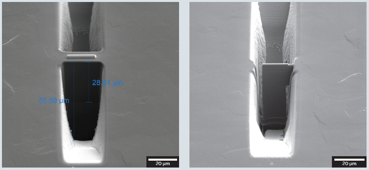
Fig. 1: Large (55 μm × 30 μm) lamella prepared in trench, shown before (left) and after (right) undercut. Image Credit: TESCAN Group
Materials and Methods
A 30 μm thick crystalline SiC layer on a Si substrate was utilized to show TEM specimen preparation and imaging of the stacking faults. TESCAN AMBER FIB-SEM equipped with TESCAN OptiLift™ nanomanipulator, with its unique position below FIB, was employed to prepare the TEM lamella.
The first step was to prepare a large (55 μm × 30 μm) lamella in trench using 100 nA (Figure 1 left) and 5 nA (Figure 1 right) beam currents, respectively.
The OptiLift™ nanomanipulator was then employed to lift out the TEM lamella (Figure 2 left), and subsequently rotate it by 100 ° to align the originally left and right sides of the lamella parallel to the TEM. The rotated lamella was attached to the Cu TEM grid, which was located at a pre-decided position on the holder (Figure 2 middle and right).
All geometrical adjustments were completed in a single step using only stage and OptiLift™ rotation and stage movement—no chamber venting was required.
Once the specimen was attached to the grid, initial polishing at a high FIB beam current distinctly revealed the SiC layer and Si substrate (Figure 3 left). Four windows, each with 10 μm width and 15 μm depth, were polished with FIB to prevent bending of the large TEM lamella.
An assumption that the polished window had a final thickness below 80 nm was made since the polished regions became transparent in SEM image at 5 keV utilizing SE detector (Figure 3). Direct imaging of the prepared TEM lamella was then completed using TESCAN’s HADF R-STEM detector at 30 keV.
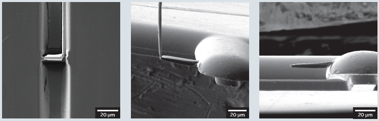
Fig. 2: TEM lamella lifted out (left), rotated by 100° (middle), and attached in single step using TESCAN OptiLift™ which facilitates a unique lift out geometry. Image Credit: TESCAN Group
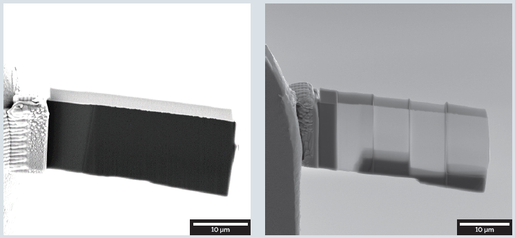
Fig. 3: TEM lamella before (left) and after (right) final polishing. Image Credit: TESCAN Group
Results and Discussion
Utilizing STEM imaging, the quality of the prepared specimen was confirmed as sufficient for characterization with STEM or TEM, which proves that FIB is applicable in the preparation of specimens with thick coatings. The STEM images demonstrate the achievement of uniform specimen transparency using the multi-window polishing approach. The large area overview image (Figure 4) shows the Si substrate, the interface, and the entire 30 μm thick layer.
The STEM image demonstrates that the stacking faults present are in much greater quantities at the interface between Si and SiC, which could be important when it comes to improving the SiC layer fabrication process. The number of stacking faults slowly declined closer to the surface of the SiC layer (from left to right in Figure 4).
Greater magnification imaging demonstrates that the stacking faults appear in several orientation planes and are mostly located right at the interface between Si and SiC. When seen from a different orientation, the inherent contrast of darkfield images showcases the stacking faults (Figure 5 right).
In Figure 6, the stacking faults can be seen in further detail, revealing different stacking faults annihilation when defects meet. For this purpose, and to gain crystallographic information, a higher keV (S)TEM would be needed. STEM in SEM in this context has been proven to successfully capture contrast from stacking faults as small as 3 nanometers in size.
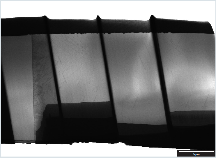
Fig. 4: STEM bright field overview image acquired at 30 keV using TESCAN’s HADF R-STEM detector in FIB-SEM. Image Credit: TESCAN Group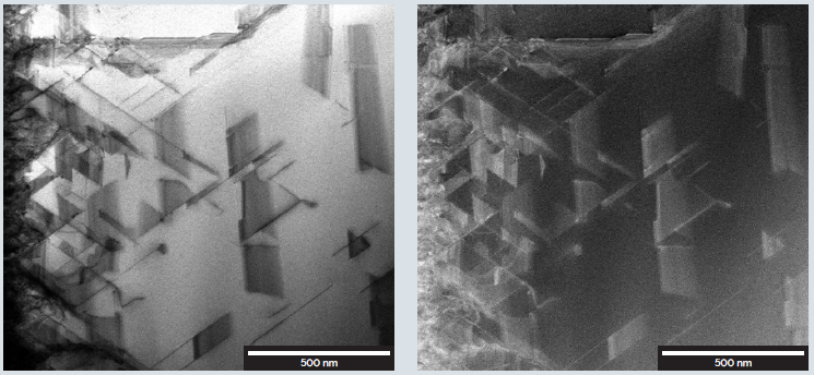
Fig. 5: Stacking faults at the interface revealed using the HADF STEM detector in FIB-SEM. Image Credit: TESCAN Group
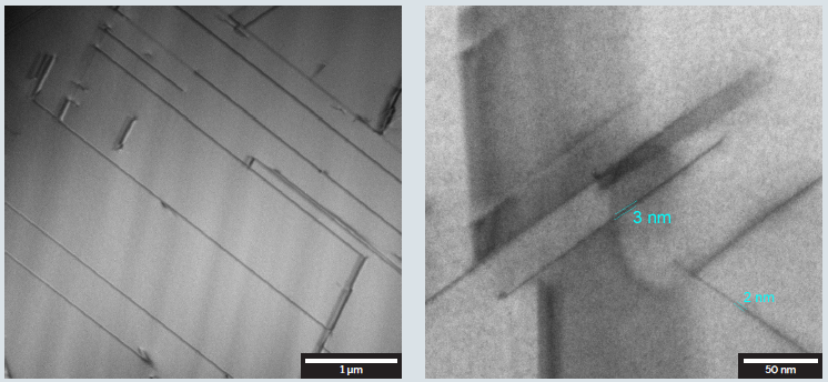
Fig. 6: Detailed image of stacking faults at the interface acquired by the HADF R-STEM detector in FIB-SEM. Image Credit: TESCAN Group
Conclusions and Outlook
This study proved that TESCAN’s unique below the FIB nanomanipulator position, in combination with TESCAN’s OptiLift™ rotating tip nanomanipulator, is irreplaceable in the performance of in-situ sample preparation from areas of interest in the 30 μm thick SiC layer.
The 100 ° rotation of the TEM lamella enabled the polishing of multiple windows at specific locations to offer a clear image of the stacking faults and their ability to develop in the layer, the substrate, and at the interface. The STEM detector imaged the stacking fault defects, offering the opportunity for both TEM lamella quality verification and detailed characterization of the stacking faults characterization at the nanoscale.
This data is useful for verifying the quality of the SiC layers or as pre-screening information for more (S) TEM imaging at high accelerating voltages in a dedicated (S) TEM like the TESCAN TENSOR.

This information has been sourced, reviewed and adapted from materials provided by TESCAN Group.
For more information on this source, please visit TESCAN Group.