Discovery and Early History of Silicon
Purity and Doping Breakthroughs
Miniaturization and the Rise of Modern Electronics
Silicon in Modern Semiconductor Technology
Sustainability and the Future of Silicon
References
Findings that Changed Practice
There was no single moment when the modern electronics era began. No switch was flipped, no machine suddenly came to life. Instead, the transformation started from the simple realization that a common material found in ordinary sand could be persuaded to behave in extraordinary ways.
Silicon is the backbone of modern electronics. It enabled the miniaturization of machines, accelerated computing, and transformed the way we live, work, and communicate.
Its true potential was realized when scientists succeeded in purifying it to near perfection and then, with atomic precision, introduced just the right impurities to control electricity. In this article, we explore how silicon evolved from a common element into the foundation of the semiconductor industry.
Saving this article for later? Download a PDF here.
Discovery and Early History of Silicon
Silicon was first isolated in 1824 by the Swedish chemist Jöns Jacob Berzelius, who reduced silica with potassium to produce a dark, brittle element.1 For decades, it remained a laboratory curiosity, valued for its chemical properties but with little practical use.
In the early twentieth century, researchers noticed something puzzling; silicon’s electrical behavior was unpredictable, sometimes conducting and sometimes resisting electricity. They realized that tiny, unintended impurities were subtly influencing its properties. This observation revealed a remarkable opportunity.
By understanding and controlling these impurities, scientists could turn silicon into a reliable material for electronics and lay the foundation for the precision and control that would define the semiconductor industry.
Purity and Doping Breakthroughs
Once scientists realized that stray atoms were discreetly shaping silicon’s behavior, the goal shifted from observation to control. The question was no longer why silicon behaved differently from one sample to another, but whether its electrical response could be intentionally designed.
In the laboratories of Bell Labs during the 1940s and 1950s, researchers began refining silicon to remove nearly every unwanted impurity, only to add back carefully chosen elements such as boron or phosphorus in vanishingly small amounts.2
This was the moment silicon became something more than a chemical element. Within a single crystal, engineers could now create regions that carried electrical charge and others that stopped it, laying the foundation for the first reliable transistor.
Over the following decades, improvements in purification and crystal growth allowed silicon to reach extraordinary purity, eventually achieving levels of 99.9999999, known as 9N. With nearly perfect crystals and precise dopants, electrons could be guided with confidence, laying the groundwork for smaller, faster, and more reliable devices.3
Miniaturization and the Rise of Modern Electronics
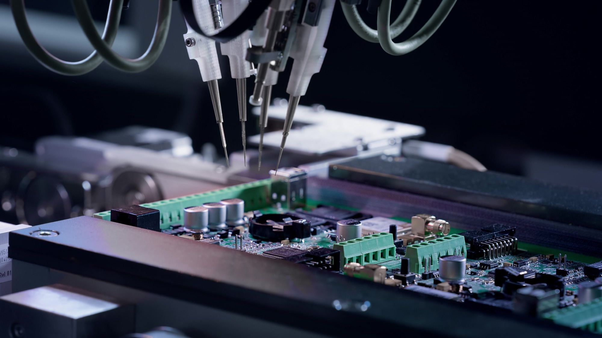 Image Credit: SibFilm/Shutterstock.com
With silicon’s electrical behavior finally under control, engineers began to ask a new question: how small could these devices become? The transistor, once demonstrated as a single laboratory component, soon became the building block of integrated circuits. By placing multiple transistors onto the same silicon chip, it became possible to perform complex electronic functions within an increasingly compact space.
Throughout the 1960s and 1970s, improvements in fabrication and material quality enabled more transistors to be packed onto a single chip without compromising performance. Each reduction in size meant faster switching, lower energy consumption, and greater computational power.
Silicon’s stability and compatibility with large-scale manufacturing enabled the replication of this process with remarkable consistency, transforming room-sized machines into desktop computers and eventually into handheld devices.
As transistors shrank from micrometers to nanometers, controlling impurities and material defects became even more critical. At these dimensions, even a few misplaced atoms could affect performance or reliability. The continued refinement of ultra-pure silicon and precise doping enabled the steady progress of miniaturization, allowing billions of transistors to be integrated into modern processors while maintaining speed and efficiency.
Like this series? Click here to learn more about the findings that have changed materials science.
Silicon in Modern Semiconductor Technology
As transistors became smaller and more powerful, silicon moved from the research laboratory into the fabric of everyday life. Today, it forms the foundation of the processors that run smartphones and computers, the memory that stores digital information, and the sensors that allow machines to interact with the world around them.
What once existed as a single transistor on a test bench is now engineered into silicon wafers containing billions of transistors working together inside modern chips.4
Silicon’s strength lies not only in its electronic properties but also in its reliability at scale. It can be grown into large, uniform crystals. This allows engineers to build complex circuits across entire wafers with consistent performance. This ability has enabled the manufacture of integrated circuits in vast quantities, powering everything from communication networks and medical devices to electric vehicles and renewable energy systems.
Even as new materials are explored for specialized uses, silicon remains the platform on which the modern semiconductor industry is built, continuing to support the technologies that shape how we compute, communicate, and generate energy today.
Sustainability and the Future of Silicon
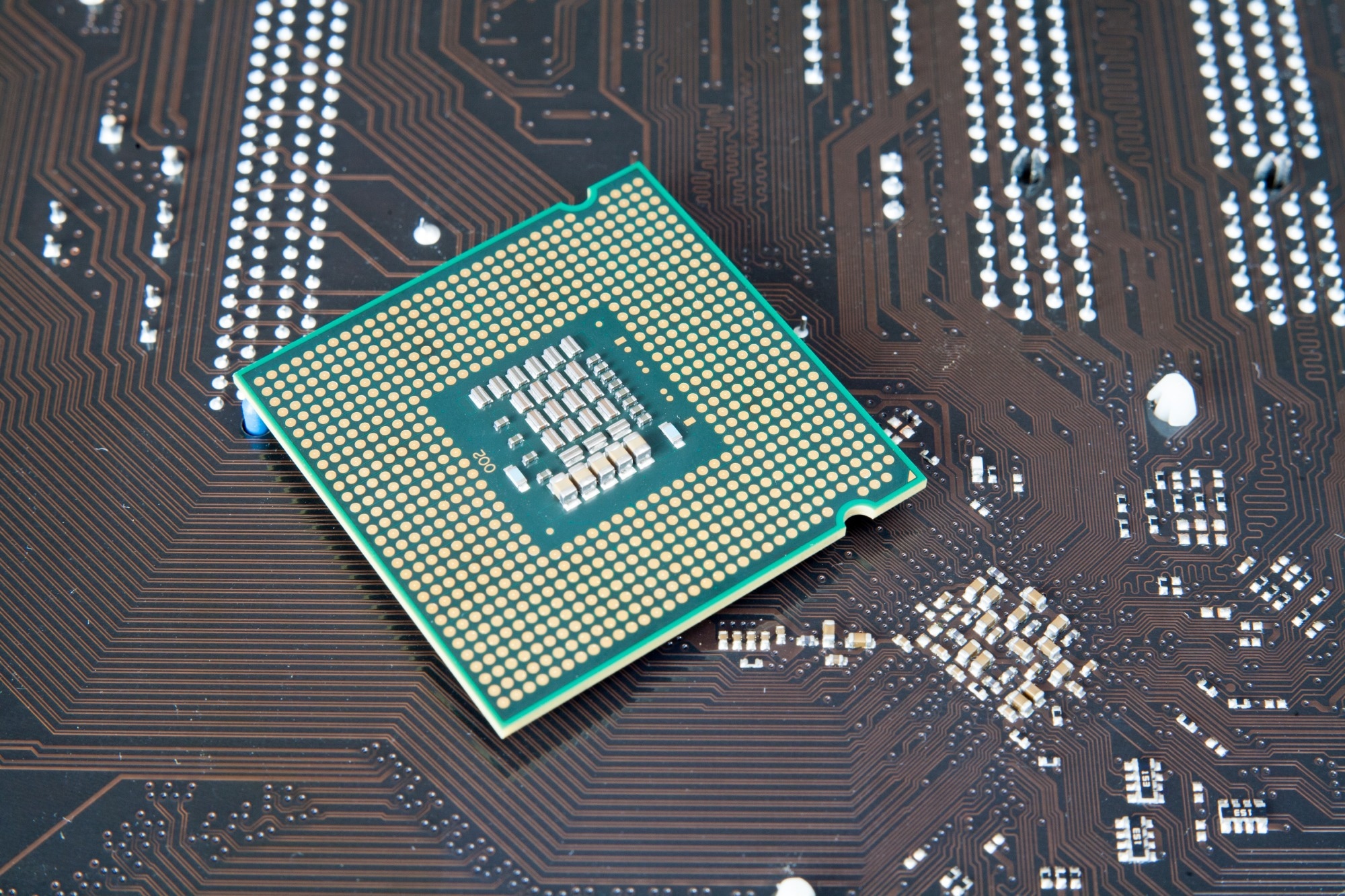 Image Credit: olvius/Shutterstock.com
After decades of rapid technological progress, silicon now faces a new challenge: supporting sustainable and energy-efficient electronics. As devices become smaller and more powerful, they also consume more energy and generate more heat.
Engineers are finding ways to use silicon more efficiently, designing chips that reduce power loss, last longer, and operate reliably under higher demands.5
Silicon’s role is also expanding beyond traditional computing. It is central to renewable energy technologies, such as solar panels and electric vehicles, where efficient power management is critical. Advances in fabrication, recycling of high-purity materials, and smarter device architectures are helping reduce the environmental footprint of semiconductor production.
Looking ahead, silicon will continue to evolve alongside emerging materials and technologies. Its ability to support smaller, faster, and more energy-conscious devices ensures that it will remain at the heart of electronics for decades to come, powering the innovations that shape how we live, work, and connect.6
References
- Royal Society of C. Silicon. Royal Society of Chemistry Periodic Table. 2023.
- Bell L. History of Semiconductor Research. Bell Labs History. 2023.
- Heywang W, Zaininger K. Silicon: the semiconductor material. Silicon: evolution and future of a technology: Springer; 2004. p. 25-42.
- Yin L, Cheng R, Ding J, Jiang J, Hou Y, Feng X, et al. Two-dimensional semiconductors and transistors for future integrated circuits. ACS nano. 2024;18(11):7739-68.
- Rogdakis K, Psaltakis G, Fagas G, Quinn A, Martins R, Kymakis E. Hybrid chips to enable a sustainable internet of things technology: opportunities and challenges. Discover Materials. 2024;4(1):4.
- Jung E. Creating the future with silicon. Advanced Materials Technologies. 2023;8(20):2200867. DOI:10.1002/admt.202200867, https://onlinelibrary.wiley.com/doi/10.1002/admt.202200867
Disclaimer: The views expressed here are those of the author expressed in their private capacity and do not necessarily represent the views of AZoM.com Limited T/A AZoNetwork the owner and operator of this website. This disclaimer forms part of the Terms and conditions of use of this website.