Mr. Bigall and his team worked on a top-notch, effective charge carrier separation method. The research paper states that the combination of noble metals and semiconductors at the nanoscale yields advantageous properties, especially for a photovoltaic industry as well as photocatalysis applications.
The performance of such a combination is highly dependent on charge carrier separation. Because of the little gap in valence energies between the conduction bands of CdSe and CdS, CdSe/CdS nanorods (NRs), they provide some charge carrier separation on their own.
Nanoparticle Gel Network
The latest study has proved that integration of the building blocks into a nanoparticle gel increases their applications in industry to a much greater extent. The distinct characteristics of the constituents are retained in nanogels. Distinct approaches for the synthesis of hybrid nanostructures have been discussed, as the classical methods have their limitations during the charge carrier separation process.
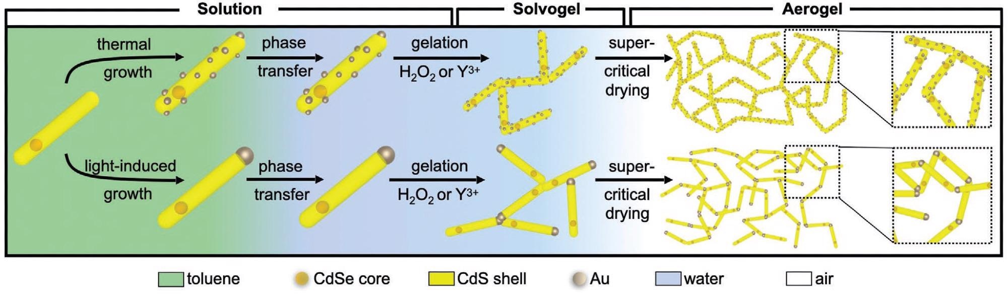
Schematic pathways from CdSe/CdS NRs to gold decorated gel networks using two different approaches. Image Credit: Schlenkrich, J. et al., Advanced Optical Materials
The primary distinction between these gels is the dramatically varying spatial separation between neighboring gold regions in hybrid nanostructures. In the present study, various gold-decorated CdSe/CdS NRs are integrated to form nano gel structures that efficiently undergo the charge separation process.
Characterization of Building Blocks
The gold decorated/tipped NRs were generated using a light-induced growth process and thermal growth process. Transmission Electron Microscopy (TEM) was performed which excitation spectrum wavelengths of 600nm and 450nm for CdSe core and CdS NR respectively.
Disparities in the range of wavelengths of 480–700 nm between the tipped-NR and random-NR systems can be explained by variations in the size of the generated gold nanostructures.
However, in hybrid particle systems, very basic scenarios resulted in the breakdown and separation of the gold domains. Within picoseconds, electrons delocalized along the CdS shell are moved to metal domains, whereas holes become situated in the CdSe core.
Upon illumination, electron delocalization may be detected throughout coupled CdSe/CdS NRs, allowing for increased electron transport to metal domains.
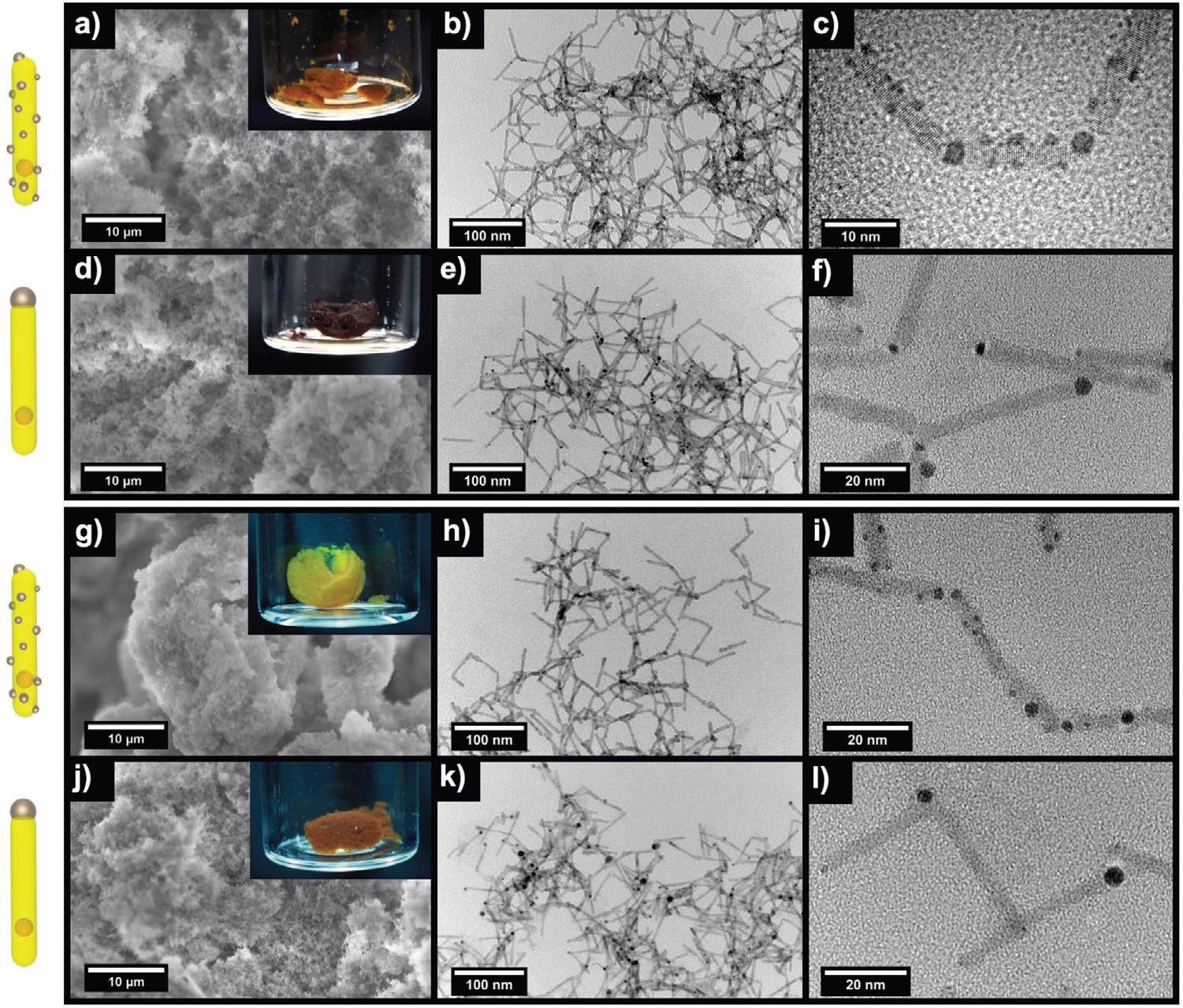
Comparative morphological overview of different hybrid aerogel networks assembled via a–f) H2O2 (upper panel) and g–l) Y3+ (lower panel). SEM images (a,d,g,j) and TEM images of random-NR aerogels assembled via H2O2 (b,c) and Y3+ (h,i) as well as tipped-NR aerogels assembled via H2O2 (e,f) and Y3+ (k,l). Insets of the SEM images show the photographs of the macroscopic aerogel monoliths. Image Credit: Schlenkrich, J. et al., Advanced Optical Materials
Structural Characterization of Nanogel
The network from NRs is synthesized mainly due to destabilizing the nanoparticles. H2O2 caused oxidation of the surface attached to Mercaptopropionic Acid (MCA). The procedure produces active sites for the synthesis, which serve as the nanorods' connecting points. A nanoparticle gel network is eventually produced in a regulated manner.
In comparison to the random-NR network, the separation between the two gold domains (ten nanometers for tipped and forty nanometers for random-NRs) and the size of the domains (3.2 ± 1.2 nanometers for tipped and 2.0 ± 0.6 nanometers for random NRs) are larger (3.2 ± 1.2 nanometers for tipped and 2.0 ± 0.6 nanometers for random NRs).
Spectrochemical Investigation of Nanogel
On xerogel samples, intensity-modulated photocurrent spectroscopy (IMPS) was used to evaluate the influence of nano-structuring on the spectro-electrochemical characteristics (charge carrier dynamics) of the hybrid macrostructures.
At bias potentials of 0 and +150 mV, positive photocurrent predominates, but at 150, 300, and 450 mV, negative photocurrent with a turnaround towards the positive photocurrent direction was observed.
The structural and optical features of the gel networks were determined by whether the hybrid particles were assembled via oxidative or ionic methods. Furthermore, the influence of various building block designs on charge carrier separation procedures was explored from a spectro-electrochemical standpoint.
Charge Carrier Dynamics
In the latest study, a model for the charge carrier dynamics was derived. When the semiconductor-metal hybrid gel networks were irradiated, the excited electrons gathered in the metal regions regardless of where the gold was located on the NRC. This is facilitated by the inherently tiny conduction band energy difference (0.23 eV) between the CdSe core and the CdS shell, which allows electron delocalization over the NR.
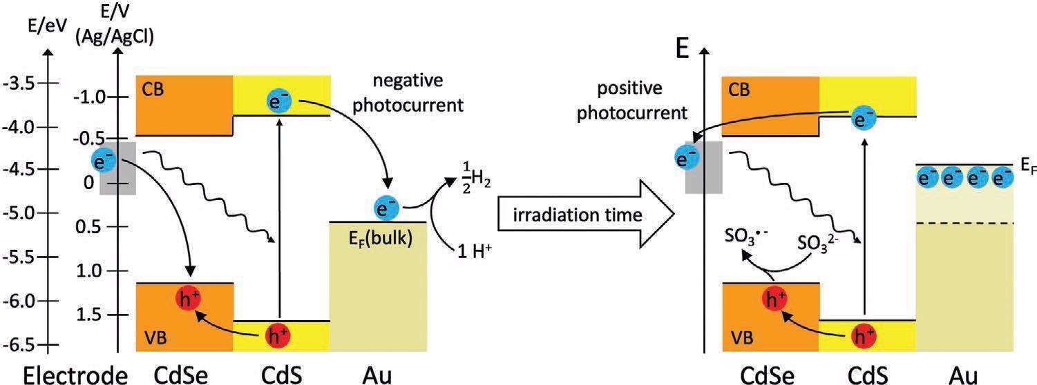
Schematic illustration of the energy landscape of the heteronanoparticle, the electron accumulation, and the rise of the Fermi level in the metal domain upon longer irradiation time and the subsequent change of the photocurrent direction. The conduction band offset at the CdSe/CdS heterojunction is around 0.23 eV, which leads to the formation of a quasi-type II alignment.For the positioning of the Au Fermi level, the bulk value was used (−5.1 eV), which can rise upon being contacted with a semiconductor surface but still remains within the bandgap of the CdS shell. Image Credit: Schlenkrich, J. et al., Advanced Optical Materials
With diminishing frequency (i.e., growing irradiation periods), the Fermi level of the gold domains rises, making electron transport from the semiconductor's conduction band to the gold domains less advantageous.
Higher photocurrent quantum efficiencies for the tipped-NR network suggest more effective charge carrier separation and hence electron transport to the electrolyte.
The tipped structures have just one Au domain on every semiconductor NR, which results in semiconductor–semiconductor contacts, allowing electron delocalization and transit over wider sections of the network.
In short, a network of nanogel particles consisting of interconnected CdSe/CdS/Au semiconductor–metal hybrid nanoparticles were prepared. The influence of the atomic distance between the metal domains on the charge carrier separation efficiency was discovered using IMP. Charge carrier separation was shown to be more successful in tipped-NR networks, leading to better negative photocurrent efficiencies as compared to random-NR networks, where charge recombination is more prominent. Truly, this novel method has made the charge separation process more efficient.
References
Schlenkrich, J., Zámbó, D., Schlosser, A., Rusch, P., & Bigall, N. C. (2021). Revealing the Effect of Nanoscopic Design on the Charge Carrier Separation Processes in Semiconductor-Metal Nanoparticle Gel Networks. Advanced Optical Materials. https://onlinelibrary.wiley.com/doi/full/10.1002/adom.202101712
Disclaimer: The views expressed here are those of the author expressed in their private capacity and do not necessarily represent the views of AZoM.com Limited T/A AZoNetwork the owner and operator of this website. This disclaimer forms part of the Terms and conditions of use of this website.