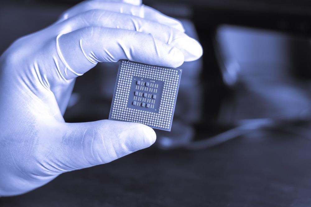
Researchers have developed a new technique to integrate multiple material devices onto a single platform via the transfer-printing (TF) technique. This article explores novel methods to develop an accurate technique to embed multiple material devices very close together in a single chip.

Image Credit: narong sutinkham/Shutterstock.com
This development is essential as it has paved an efficient way to manufacture condensed embedded single-chip devices, occupying less volume and working with greater efficiency.
Photonic Integrated Circuit (PIC)
Recently, this technology has been implemented for industrial purposes. Classical PIC manufacturing technique was based on single-material manufacturing. However, the latest research has made it clear that to efficiently perform multiple optical and electronic functions, an embedded system of multiple materials is an essential requirement.
This is the core reason the novel research is based on the incorporation of various types of materials on a single chip platform.
Materials and Methods
Transfer printing has been utilized in a study in the journal Optical Materials Express resulting in a chip size easily compatible with the size of the intended device. Two dense device integration implementations employing transfer printing are given. The first one is the micro-disk resonator while the second one is the nanowire laser method.
The micro-disk resonator involves µ-disk resonators integration in AlGaAs and diamond materials with a GaN-on-Sapphire waveguide platform. The diamond, AlGaAs, and GaN waveguide devices were all made separately and then combined using the transfer print process.
Tackling the Chip Shortage with the Semiconductor Circular Economy
Electron beam lithography was implemented for the pattern creation of three chips. The thickness of single-crystal diamond was reduced to 1.8 µm. The printing experiments utilized two discs whose diameters were 10 µm and 20 µm.
The second method was the nanowire (NW) lasers. It consisted of NW lasers, with a device separation of 1 µm. The NW lasers used were InP NW lasers. An average laser length of 5 and 10 µm with average diameters of 435 and 260 µm were utilized for this purpose. The cross-sections were hexagonal. The core/shell GaAs/AlGaAs NW lasers diameter and length were ∼ 450 nm and ∼ 4 µm, respectively.
Because the NW devices have a sub-µm short axis dimension and a targeted m scale spacing, the PDMS stamp will be interfaced with pre-printed devices throughout successive printing.
Classic Industrial Utilization
As mentioned above, classically only single material was used for this purpose. This single material platform was synthesized with the deposition of other materials such as SiN. The major advancement and research were due to its vast utilization in industries such as hybrid optical platforms, the telecommunication industry, IOT Industry, and quantum photonic applications.
Limitations
Although the technology has some massive advantages, a few challenges are still to be overcome for its implementation. A major issue is the complex coupling of numerous diverse semiconductor electronics in a small footprint to make optimum use of chip area and integrate a variety of functionalities into a single chip.
When electronics are printed via transfer printing, the stamp comes into immediate contact with the receiver. As a result, in processes with several printing stages, tightly packed devices will react with the stamp material, with the possibility of device ejection or change in place.
Latest Findings
The micro-disk resonator experiments showed all footprints within 50 X 120 µm2. A modest distributed loss of 3.13 dB/cm, proportional to a high intrinsic Q factor of 122,000, is also measured. The waveguide spectra were measured in the 1540 - 1600 nm range using an end-fire transmission system.

Image Credit: narong sutinkham/Shutterstock.com
The edge and vertical linked devices were found to have an average Q-factors of 14,000 and 7,600, respectively. The vertically connected diamond disk was discovered to have a Q-factor of 91,000.
As for the NW laser process, two NWs with similar lasing wavelengths (850 nm) from the same material platform (InP) were employed. Using both GaAs/AlGaAs (750 nm) and InP (850 nm) devices in a single pair, a larger lasing wavelength spread between two devices was then accomplished. The differences were then measured as the centroid-to-centroid spacing of the NWs using SEM images and found to be within 188 nm of the intended values.
Future Industrial Applications
The novel technology would find rapid utilization for various industries such as flexible digital x-ray detectors, bio-integrated neural electrode arrays, and digital x-ray detectors. The wide range of industries that would benefit from this includes energy-harvesting devices, light-emitting diodes, solar cells, flexible capacitors, and many more.
Process Complexities
Although research such as this has shown the advantages of these processes, many complexities fundamentally make this very intricate. High temperature and pressure are basic requirements. The production speeds are also lower, owing to limited dyestuff. The process does not apply to all types of fibers too; a strong fiber capable to withstand high temperature and pressure is needed.
Future Perspective
The experts are now aiming to duplicate these findings with a bigger variety of devices to demonstrate that it is functional at a broader scale. They also intend to integrate their transfer printing method with an autonomous implementation phase of the project they previously created to allow for the quick evaluation, identification, and transfer of hundreds of discrete devices for scanning and hybrid optical circuits technologies.
In short, the printing technique has been successful in integrating components of several materials on a single chip very close together. The printing is not only applicable for optical systems; rather, a huge potential exists for electronics systems. Truly, this novel technique has been a great discovery, modifying the manufacturing techniques in chip manufacturing.
Fast Scanning Chip Calorimetry: Possibilities and Applications
References
Jevtics, D., Smith, J. A., McPhillimy, J., Guilhabert, B., Hill, P., Klitis, C., . . . Strain, M. J. (2021). Spatially dense integration of micron-scale devices from multiple materials on a single chip via transfer-printing. Optical Materials Express, 3567-3576. https://www.osapublishing.org/ome/fulltext.cfm?uri=ome-11-10-3567&id=459987
Linghu, C., Song, J., Wang, C., & Zhang, S. (2018). Transfer printing techniques for flexible and stretchable inorganic electronics. npj Flexible electronics. https://www.nature.com/articles/s41528-018-0037-x
Zhou, H., Qin, W., Yu, Q., Cheng, H., Yu, X., & Wu, H. (2019). Transfer Printing and its Applications in Flexible Electronic Devices. Nanomaterials. https://www.ncbi.nlm.nih.gov/pmc/articles/PMC6410120/
Researchers integrate optical devices made of multiple materials onto single chip (2021, September 29) retrieved 5 November 2021 from https://phys.org/news/2021-09-optical-devices-multiple-materials-chip.html
Disclaimer: The views expressed here are those of the author expressed in their private capacity and do not necessarily represent the views of AZoM.com Limited T/A AZoNetwork the owner and operator of this website. This disclaimer forms part of the Terms and conditions of use of this website.