|
Amorphous solids, like common glass, are materials in which the atoms are not arranged in any particular order. They do not form crystalline structures at all, and they contain large numbers of structural and bonding defects.
It wasn't until 1974 that researchers began to realize that amorphous silicon could be used in photovoltaic (PV) devices by properly controlling the conditions under which it was deposited and by carefully modifying its composition. Today, amorphous silicon is commonly used for solar-powered consumer devices that have low power requirements (e.g., wrist watches and calculators).
Amorphous silicon absorbs solar radiation 40 times more efficiently than does single-crystal silicon, so a film only about 1 micron (one one-millionth of a meter) thick can absorb 90% of the usable solar energy. This is one of the most important factors affecting its potential for low cost. Other principal economic advantages are that amorphous silicon can be produced at a lower temperature and can be deposited on low-cost substrates. These characteristics make amorphous silicon the leading thin-film PV material.
A Closer Look
Because amorphous silicon does not have the structural uniformity of crystalline or even polycrystalline silicon, the small deviations result in defects such as dangling bonds, where atoms are missing a neighbour to which they can bond. These defects provide places for electrons to recombine with holes rather than contributing to the electrical circuit. Ordinarily, such a material would be unacceptable for electronic devices because the defects limit the flow of current. But if amorphous silicon is deposited in such a way that it contains a small amount of hydrogen (through a process called "hydrogenation"), then the hydrogen atoms combine chemically with many of the dangling bonds, essentially removing them and thereby permitting electrons to move through the amorphous silicon.
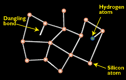
Figure 1. - Amorphous silicon's random structural characteristics result in deviations like "dangling bonds." Dangling bonds provide places for electrons to recombine with holes, but this may be neutralized somewhat with hydrogen.
Cell Design
Because of amorphous silicon's unique properties, the cells are designed to have an ultrathin (0.008-micron) p-type top layer; a thicker (0.5- to 1-micron) intrinsic (middle) layer; and a very thin (0.02-micron) n-type bottom layer. The top layer is made so thin and relatively transparent that most incident light passes right through it, to generate free electrons in the intrinsic layer. The p and n layers (produced by doping amorphous silicon) create an electric field across the entire intrinsic region to induce electron movement in that layer.
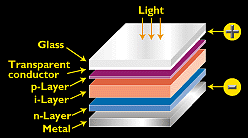
Figure 2. - The typical amorphous silicon cell employs a p-i-n design, in which an intrinsic layer is sandwiched between a p layer and an n layer.
|