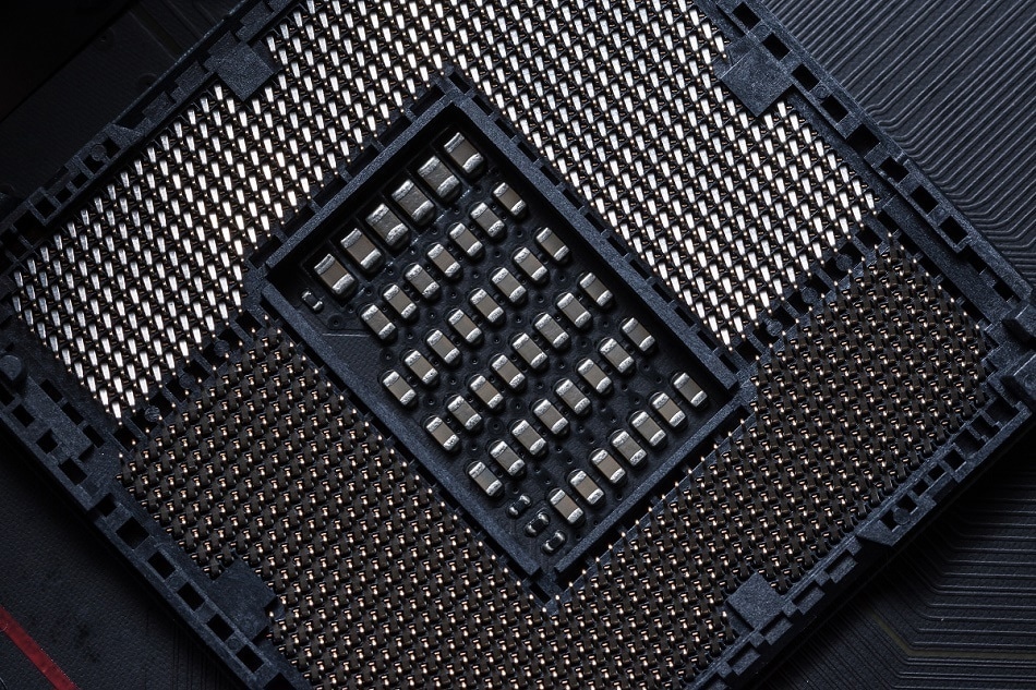
The demands of processing speed in microelectronics is pushing the industry to develop smaller and more advanced chip architectures. The nanoscale features on modern chips are difficult to reliably analyse using conventional methods, which struggle to attain the resolution levels required. FIB delayering using xenon plasma has been shown to be a solution to this problem.
Consumer applications are demanding high performance, low energy consumption, a decreased device foot-print and lower production costs.The microelectronics industry, as ever, has to be ahead of the game, and this has led to a growing density of the elements in microelectronics and shrinkage of the elements to the nanometre scale. Packing more into a smaller space and also decreasing the component scale has delivered a new set of challenges for both production technology and failure analysis in these devices. Current commercial electronics are based on 22 nm and 14 nm node technology. However, the next generation of 10 nm and 7 nm nodes are now under development and the industry needs reliable methods in place for testing and failure analysis.
The Use of Delayering in Failure Analysis
Delayering or de-processing is essential in testing for physical defects in integrated circuit layers (ICs). Delayering involves the removal of a devices surface, layer by layer, to gain understanding of the properties and composition of the entire device. This could be compared to making measurements throughout a cross section of the device.
Historically, delayering has been carried out using wet chemical methods, reactive ion etching or mechanical manual polishing. However, many of these methods suffer from drawbacks that make them unsuitable for sub-20 nm manufacturing.
For example, manual polishing is difficult to control and stop in the correct layer, and may also introduce defects into the sample. Reactive ion etching is also difficult to control and there is a conflict between the etching rate and anisotropic profile. Other chemical or plasma methods can problematically leave residues which alter the physical and chemical properties of the sample, interfering with the accuracy of subsequent tests. Ultimately, as process nodes scale to ever smaller sizes, successfully controlling front side manual de-processing with older techniques is increasingly challenging. The reasons for this include:
- Smaller critical dimensions of the transistor and the Back-end-of-line (BEOL) metal interconnect features
- A reduction in the thickness of the dielectrics
- New porous ultra-low k materials
Xe Plasma FIB for the Failure Analysis of Nanoscale Layers
Gas assisted Xe plasma focused ion beam (FIB) technology is a proven, reliable method for the testing of sub-20 mm technology features of testing sub-20 mm technology features. This technology is ideal for the uniform delayering of metal and dielectric layers. FIB is accurate and controllable enough to target a failure with nanometre accuracy in both depth and lateral directions.
Xe FIB is a powerful technique for the removal of the metallic surface (de-processing) of heterogenous materials such as microelectronic systems. Deprocessing provides a planar surface area which can then be tested further by contact or optical microscopy.
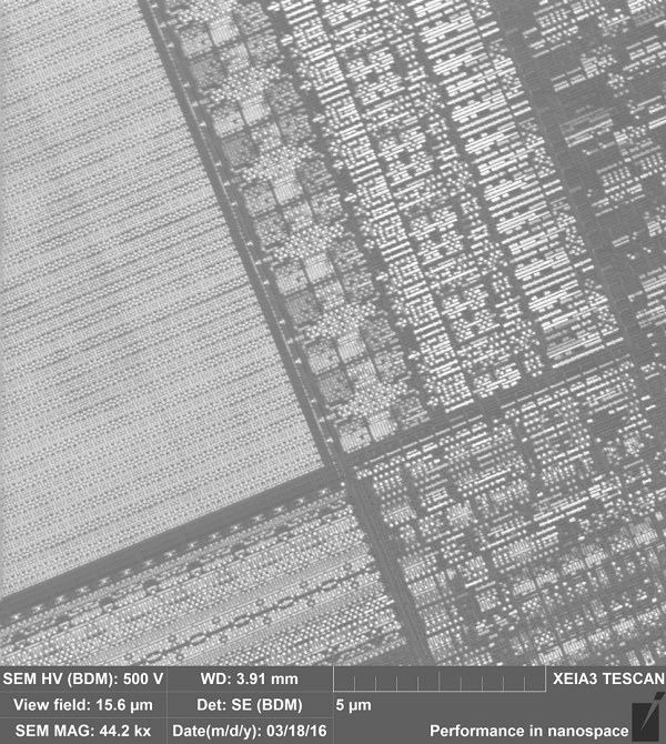
A deprocessed microelectronics chip imaged using SEM
Xe FIB can provide uniform planarity on each de-processed layer of microelectronics - from the thicker metal layers on the external face of a device, to the thin transition layers inside the device. This allows each layer to be inspected and examined in a site-specific layer-by-layer excavation). Due to the precise control the Xe-FIB system affords, researchers can de-process a sample to reach specific layers of interest which can then be further inspected.
The Benefits of TESCANs Xe Plasma FIB for Failure Analysis
TESCAN Xe plasma FIB system is ideal for the de-processing of semiconductors for failure analysis and fault isolation. Unlike in methods such as wet etching or polishing microelectronic chips retain functionality as each layer is removed during the testing process. The process uses a gas-assisted delayering technique which combines Xe plasma FIB with suitable gas chemistry to allow planarity, even where delayering is a problem due to variance in milling rates between insulator and thick metal layers. This means that layer intermixing is minimized.
Gas-assisted delayering can also be used through all metal layers throughout the entire chip. This is ideal for delayering uniformly through the smallest structures, which is especially good for sub-20 nm process nodes. Electrical probing can be performed in-situ for fault isolation.
The TESCAN method provides large-area windows (100 µm × 100 µm) at site-specific locations with minimal surrounding effects for high throughput delayering and analysis. Xe plasma FIB is a particularly powerful technique when combined with a scanning electron microscope column (FIB-SEM).
This provides a highly suitable system for accurate end-point detection and for monitoring the delayering process. The end-point detection is achieved as a combination of SE signal collection during the initial delayering steps and observation of the delayering and low-kV SEM imaging in the final steps. The whole point of the process is to provide a delayered surface ready for nanoprobing without obstruction such as oxide layers, mechanical damage, or any intermixed layers.
Why Xenon FIB is Advantageous over Gallium for Chip Delayering
In Ga-FIB based techniques Ga metal can be implanted into the material during the milling process. The advantage of Xe-FIB is that Xe gas does not form metallic compounds that alter the conductivity of the samples or produce metallic bridges.
Ga-FIB sources are not suitable for IC delayering because Ga implantation changes the conductivity of the surface and subsequent electrical tests are not reliable. In addition, Xe ions considerably reduce surface amorphisation when compared to Ga ions.
TESCAN’s XEI3 for Nanoscale Electronics Analysis
TESCAN combines a Xe plasma FIB column with ultrahigh-resolution SEM columns such as the TESCAN XEIA3 to allow high-resolution SEM imaging with excellent performance at low beam energies. This type of system is ideal for imaging the fragile low-k dielectric layers that are exposed following delayering.
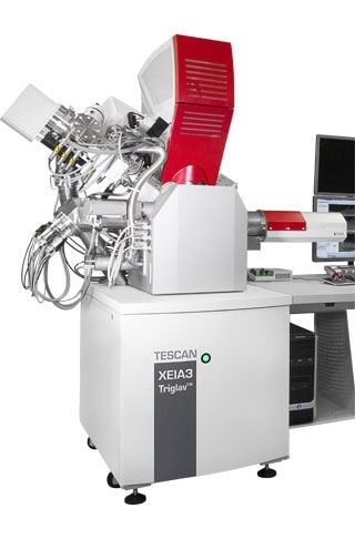
The XEIA3 from TESCAN
This imaging is usually carried out at < 500 eV in order to minimise the risk of beam damage on transistors and to be able to resolve features of only a few nanometres. However, the versatility of the Xe plasma FIB is also worth mentioning. The system offers a large ion beam current range allowing a wide range of applications in one instrument.
Download the Brochure for More Information
The large currents permit fast milling rates for removal of larger-volume bulk material. The medium currents are ideal for large-volume FIB-tomography. And ultimately the low currents can be purposed for TEM lamella polishing and delayering. Finally, ultra-low currents are excellent for damage-free polishing and nanopatterning.
References
- V Viswanathan, S Sharang, D Zudhistir et al., Precision Xe Plasma FIB Delayering for Physical Failure Analysis of sub-20 nm Microprocessor Devices, 43rd International Symposium for Testing and Failure Analysis (November 5-9, 2017)
- Jozef Vincenc Oboňa, Tomáš Hrnčíř, et al., Xe plasma FIB Delayering of IC based on 14 nm node technology, Microsc. Microanal. 22 (Suppl 3), 2016, p56-57
- Bruce K. Gale, Dry Etching: Fundamentals of Micromachining, Lecture BIOEN 6421, University of Utah
- J. V. Oboňa et.al., Delayering of 14 nm Node Technology IC with Xe Plasma FIB, Eur. Micro. Cong. Proc, 2016
- Sharang et. al., Xe Plasma FIB based Delayering for Physical Failure Analysis of 14 nm Device Technology, European FIB Network Workshop, 2017
TESCAN Group
Founded in 1991 by a group of managers and engineers from Tesla with its electron microscopy history starting in the 1950’s, today TESCAN is a globally renowned supplier of Focused Ion Beam workstations, Scanning Electron Microscopes and Optical Microscopes. TESCAN’s innovative solutions and collaborative nature with its customers have won it a leading position in the world of nano- and microtechnology. The company is proud to participate in premier research projects with prominent institutions across a range of scientific fields. TESCAN provides its clients with leading-class products in terms of value, quality and reliability. TESCAN Group is the North American arm of TESCAN Group, a multinational company established by the merger of Czech company TESCAN, a leading global supplier of SEMs and Focused Ion Beam workstations, and the French company ORSAY PHYSICS, a world leader in customized Focused Ion Beam and Electron Beam technology.

This information has been sourced, reviewed and adapted from materials provided by TESCAN Group.
For more information on this source, please visit TESCAN Group.