For advanced electronics such as photovoltaics, even subtle distortions in crystal structure are crucial to performance. Analysis of these materials must take place on the smallest of scales, often in specific locations, taking into account variations in crystal structures and their distributions within a material.
Transmission Electron Microscopy (TEM) has proved to be one of the most powerful techniques for the nanoscale structural characterization of semiconductor materials. The high spatial resolution of TEM allows the imaging of nanoscale structural features and atomic positions so even the smallest defects and crystal distortions can be identified. However, the technique is very region specific and specimen volumes examined are tiny, often only a few cubic microns.
This means that, prior to TEM imaging, the nanoscale area to be studied must be carefully located within the larger sample. Additionally, once identified, the region of interest must also be prepared for TEM. This is often carried out by FIB milling, which can be used to extract a sample of suitable thinness for TEM imaging from a very specific location in a material.
Consequently, the use of good secondary analysis techniques to locate the specific region of interest in conjunction with focused ion beam (FIB) to prepare the site for analysis is essential. Often, Electron Back Scatter Diffraction (EBSD) and Energy-Dispersive X-ray Spectroscopy (EDS) have been used to locate variations in crystal structure which are indicative of the area of interest to be imaged. However, if the differences in crystal structure and composition are too small these techniques cannot be used. In these cases, a new correlative microscopy technique called Raman Imaging-Scanning Electron (RISE), which is highly sensitive to bonding differences within a sample, can be used.
RISE Correlative Microscopy
RISE microscopy is a novel correlative microscopy technique which combines scanning electron microscopy (SEM) and confocal Raman imaging for improved secondary analysis. The Raman element of RISE Microscopy provides the ability to distinguish between very small differences in bonding, facilitating the detection of even the smallest chemical and structural differences in a sample.
RISE allows researchers to correlate ultra-structural surface properties to a sample’s molecular constitution. For example, RISE allows the differences in bonding that result from crystal dislocations or polymorph formation to be understood.
RISE microscopes can easily switch between Raman and SEM imaging, and the two images can also be correlated with each other to display structural and chemical information in one single correlative image. Once the area of interest has been located a specimen can be extracted using an FIB system for further analysis by TEM.
The Different Polymorphs of Titanium Dioxide
Titanium dioxide (TiO2) thin films are important in photoelectrochemical (PEC) applications where they are often used to form semiconductor heterojunctions with materials such as silicon carbide. The polymorphic form of the titanium dioxide used in microelectronic structures can impact performance so correlative Raman microscopy, such as RISE, can help researchers optimize devices.
Titanium dioxide displays three different polymorphic forms - rutile, anatase, and brookite, which all possess different levels of electrical conduction. Anatase forms in a tetragonal structure with corner-sharing octahedra. Brookite is slightly distorted from anatase into an orthorhombic structure and displays both corner- and edge-sharing octahedra.
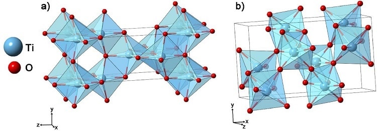
Figure 1: Diagram illustrating the different crystal structures of the titanium polymorphs anatase (a) and brookite (b) Source - Ultramicroscopy
The distortion between the two forms is subtle, meaning structural variations between brookite and anatase polymorphs of TiO2 are difficult to detect. Their identical chemical compositions and similar diffraction patterns mean that neither EDS nor EBSD are sufficient for differentiating between brookite and anatase. There is, however, variation in the Ti–O bonding between the two polymorphs. This means measurable differences in vibrational modes of the bonding within each structure allows Raman spectroscopy to distinguish between the two polymorphs.
Using RISE to Study Variations in Polymorph Distribution
A study of titanium dioxide polymorphs was conducted on thin film samples containing both brookite and anatase. The goal was to prepare a sample and examine the boundary between the two polymorphs. The film was first imaged using SEM to identify a region of interest. Then, using a confocal Raman imaging system integrated with the SEM (RISE), a 100 × 100 spectral array was generated by collecting and assembling single spectra within the region of interest.
Following background correction, a cluster analysis was performed on the 2-D spectral array. Two main clusters of Raman spectra were identified which corresponded to the brookite and anatase phases. The 2-D spectral arrays resulted in four distribution images of the identified chemical/structural species. These images could even distinguish between the orientation of the brookite and the porosity of the anatase phases.
Using the frequency variations of the spectra, a color-coded Raman image was generated, showing the distribution of the titanium polymorphs in the selected area. Overlaying the Raman image on the SEM micrograph allowed the precise location of each polymorph to be identified (figure 2) and tracked for TEM preparation.
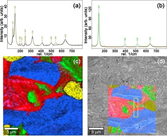
Figure 2: Raman spectra for brookite (a) and anatase (b). A color-coded Raman image (c) is overlaid with SEM images showing the distribution of polymorphs within a sample (d). The yellow box in (d) indicates the region of interest selected for further TEM analysis. Source - Ultramicroscopy
FIB was then used to prepare a thin cross-section of the film containing a boundary between regions of brookite and anatase. Finally, dark field TEM imaging was conducted (figure 3) to confirm the presence of the boundary between the two polymorphs.
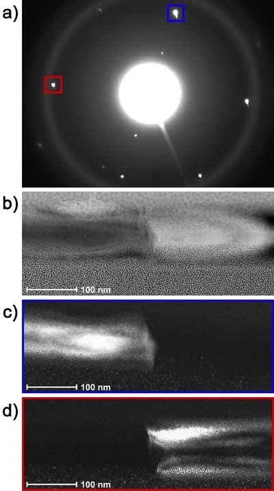
Figure 3: (a) Diffraction pattern showing polymorph specific regions with brookite in blue and anatase in red, (b) bright field image, (c) dark field of the brookite region and (d) dark field of the anatase region. Source - Ultramicroscopy
The S8000G FIB-SEM from TESCAN
The correlative imaging technique termed RISE microscopy was introduced by TESCAN and WITec in 2014. The integration of a confocal Raman microscope into an FIB-SEM workstation allows the acquisition of Raman and electronic images of the same area within the same instrument. This configuration is well-suited to distinguish between polymorphs with similar structures and chemistries. This capability provides a new tool for the analyst for Raman active materials including ceramics, semiconductors, organics, biomaterials, and even geologic materials.
The TESCAN S8000G is the newest focused ion beam scanning electron microscopy (FIB-SEM) system on offer. In combination with Raman spectroscopy this provides the ideal RISE capabilities in one instrument. The TESCAN S8000G is also equipped with a BrightBeam™ SEM column for field-free ultra-high-resolution imaging, and the novel Orage™ Ga FIB column with improved resolution and performance at low beam energies.
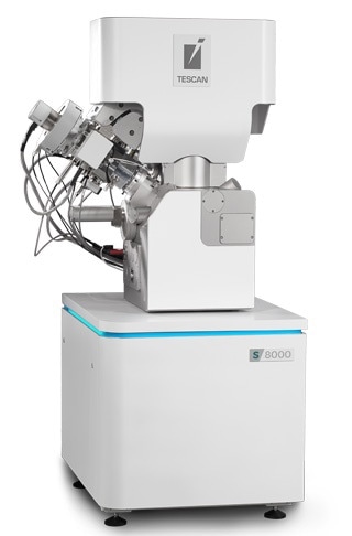
The S8000G from TESCAN
A correlative approach using Raman spectroscopy for targeted focused ion beam specimen preparation can just as easily be employed in producing specimens for atom probe tomography or even micropillar nanoindentation of heterophase materials.
Download the Brochure for More Information
References and Further Reading
- John S. Mangum, Lisa H. Chan, Ute Schmidt, Lauren M. Garten, David S. Ginley, Brian P. Gorman, Correlative Raman spectroscopy and focused ion beam for targeted phase boundary analysis of titania polymorphs, Ultramicroscopy 188 (2018) 48–51
- R.S.Pesso, M.A.Fraga et al., Nanostructured thin films based on TiO2 and/or SiC for use in photoelectrochemical cells: A review of the material characteristics, synthesis and recent applications, Materials Science in Semiconductor Processing, Volume 29, January 2015, Pages 56-68
- B. Fultz & J. M. Howe, Transmission Electron Microscopy and Diffractometry of Materials, Springer-Verlag Berlin Heidelberg, 2013, 764 pages, ISBN 978-3-642-29761-8
TESCAN Group
Founded in 1991 by a group of managers and engineers from Tesla with its electron microscopy history starting in the 1950’s, today TESCAN is a globally renowned supplier of Focused Ion Beam workstations, Scanning Electron Microscopes and Optical Microscopes. TESCAN’s innovative solutions and collaborative nature with its customers have won it a leading position in the world of nano- and microtechnology. The company is proud to participate in premier research projects with prominent institutions across a range of scientific fields. TESCAN provides its clients with leading-class products in terms of value, quality and reliability. TESCAN Group is the North American arm of TESCAN Group, a multinational company established by the merger of Czech company TESCAN, a leading global supplier of SEMs and Focused Ion Beam workstations, and the French company ORSAY PHYSICS, a world leader in customized Focused Ion Beam and Electron Beam technology.

This information has been sourced, reviewed and adapted from materials provided by TESCAN Group.
For more information on this source, please visit TESCAN Group.