Nanocrystalline diamond is grown by chemical vapor deposition. It is generally grown on substrates such as silicon wafers, forming a solid film of nano-sized diamond particles with diverse applications in nanotechnology.
Nanocrystalline Diamonds
These nanocrystalline diamonds offer the more practical properties of diamond – in particular, its hardness – but at considerably lower costs. Nanocrystalline diamonds are suitable for an assorted range of applications due to their toughness, hardness, and surface stability, but it is vital that these are characterized appropriately in order to make the best use of their specific properties.
TESCAN S8000 Microscope
One such device which can ensure appropriate characterization of nanocrystalline diamonds is the TESCAN S8000 microscope. It is fitted with a BrightBeam™ SEM column and offers a reliable, sturdy detection system made up of in-chamber BSE and E-T detectors, working alongside powerful in-beam detectors with energy-filtering and angle-selective capabilities.
The BrightBeam™ SEM column technology is able to offer field-free ultra-high resolution using a combined electrostatic-magnetic objective lens design. These types of electron optics have been developed to provide outstanding performance, especially when working at low beam energies.
This impressive combination of features combines to provide high spatial resolution, first-class image contrast, and the amount of surface sensitivity required to effectively resolve the nano-sized structures present in nanocrystalline diamonds.
Electron signals that are collected by the detection system can be acquired at the same time, then combined to allow the maximum level of insight into the sample in question.
Total Control over Surface Sensitivity
Additionally, this detection system gives the user total control over surface sensitivity, meaning that the option to explore different contrasts is now much more viable and achievable; examining the sample from pure topographic or material properties, or a combination of both.
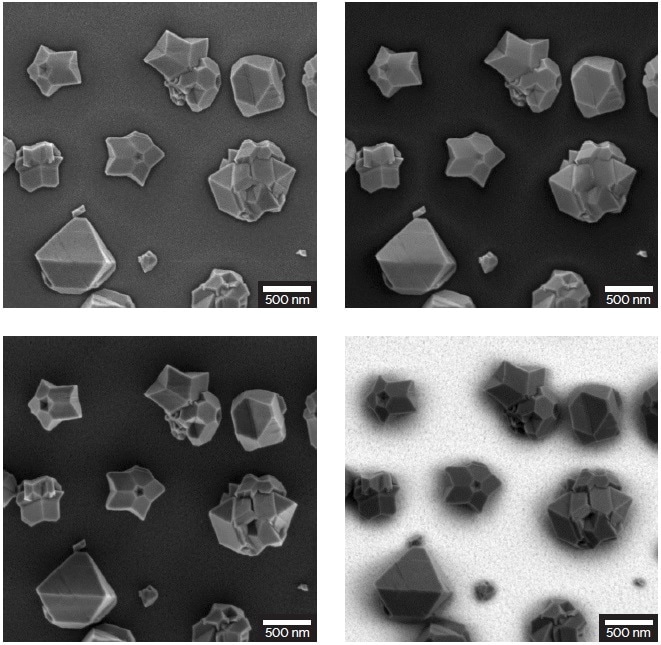
Figure 1. Fault planes and complex geometries of individual particles in nanocrystalline diamonds on Si substrate acquired at 2 keV with the four detectors Multidetector (top left), Axial detector (top right), E-T detector (bottom left) and BSE detector (bottom right).
TESCAN Group
Founded in 1991 by a group of managers and engineers from Tesla with its electron microscopy history starting in the 1950’s, today TESCAN is a globally renowned supplier of Focused Ion Beam workstations, Scanning Electron Microscopes and Optical Microscopes. TESCAN’s innovative solutions and collaborative nature with its customers have won it a leading position in the world of nano- and microtechnology. The company is proud to participate in premier research projects with prominent institutions across a range of scientific fields. TESCAN provides its clients with leading-class products in terms of value, quality and reliability. TESCAN Group is the North American arm of TESCAN Group, a multinational company established by the merger of Czech company TESCAN, a leading global supplier of SEMs and Focused Ion Beam workstations, and the French company ORSAY PHYSICS, a world leader in customized Focused Ion Beam and Electron Beam technology.

This information has been sourced, reviewed and adapted from materials provided by TESCAN Group.
For more information on this source, please visit TESCAN Group.