Organic light emitting diodes (OLEDs) — a flat light emitting technology — comprise of a series of organic thin films arranged between two conductors. They emit bright light when an electrical current is applied. Since OLEDs are emissive displays that eliminate the need for a backlight, they are more efficient and thinner when compared to LCD displays (which need a white backlight).
Another benefit of OLED displays is that they are flexible. Consequently, OLED technology has recently been very prevalent in the present-day display market. At present, OLED displays are mass-produced for tablets, mobile phones, wearables, and TVs.
OLED or AMOLED Display
The Active Matrix OLED or AMOLED display is one type of OLED display that has a back panel of thin-film transistors, an attribute that renders pixel control easier and more accurate. It is this feature that makes AMOLED technology ideal for large-size displays. In comparison with traditional glass-based displays, plastic AMOLED panels are much lighter and thinner, allowing either larger batteries or thinner devices. Furthermore, next-generation flexible displays will make foldable mobile devices possible. At present, the two chief segments are smartphones and wearable devices such as smartwatches. However, with the advancement in technology, the use of those displays in other applications, like automotive displays, will be possible.
Physical failure analysis of OLED/AMOLED displays can be highly complex because of the presence of an extensive range of materials such as ITO, polyimide, organic layers, glass, Al electrodes, and other metals with physical properties varying substantially from each other. These materials are arranged in the form of very thin films with thicknesses that vary even in the nanometer scale.
An established method to check for failures in displays is preparing cross-sections at particular locations on the display, thereby allowing the detailed examination of these multi-layered structures. Subsequently, the cross-sections are examined using high-resolution scanning electron microscopy imaging, which enables such thin layers to be resolved to find possible manufacturing artifacts or flaws that result in display malfunction.
A standard method for preparing cross-sections in displays is the use of mechanical polishing. Although this technique allows large-area cross-sections to be quickly prepared, it has several limitations, such as inducing severe artifacts like tearing, mechanical stress, delamination, or even the total destruction of a part of the display.
The TESCAN S9000X is a Xe plasma focused ion beam scanning electron microscope that has it all for preparing large-area cross-sections in displays that can be as large as 1 mm wide, and at the same time offers high resolution and exceptional contrast at low beam energies needed to image and resolve such small and delicate structures in displays. In terms of sample modification, the S9000X comes with the new iFIB+™ Xe plasma FIB column with the potential to realize a very large field of view with no match in the market (1 mm at 30 keV), a key feature that — in combination with the high milling rates at high ion beam currents that are possible with Xe plasma FIB — allows the preparation of extra-large cross-sections in displays (and in other large structures such as MEMS, TSVs, BGAs, and so on).
Thus, the TESCAN S9000X can be used to easily prepare 1 mm wide, high-quality and artifact-free cross-sections within a matter of hours, something which can never be achieved using traditional Ga FIBs. With regards to imaging, the next-generation Triglav™ ultra-high-resolution SEM column is provided with an enhanced in-beam detection system with extended detection capabilities (energy-filtering axial BSE signal detection) offering superior contrast and improved sensibility, specifically at low beam energies, which is necessary to resolve nano-sized features and thin layers in displays.
Illustrated in Figure 1 is a 187 µm deep, 1086 µm wide cross-section prepared at an ion beam current of 2 µA and a beam energy of 30 kV. The in-column Mid-Angle BSE detector offers high-contrast images of the metallic layers inside the display (Figure 2 and Figure 3).
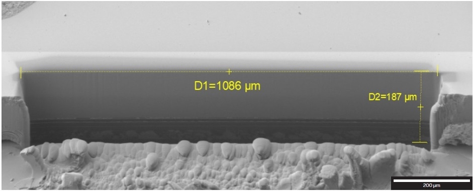
Figure 1. 1086 µm wide cross-section through part of an OLED display, SE detector at 2 kV.
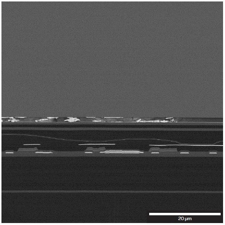
Figure 2. Detailed image of the vertical structure of the part of OLED display—top passivation/Al electrodes/polyimide/ITO/polyimide. Mid-Angle BSE detector at 2 kV.
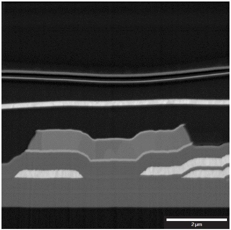
Figure 3. Detailed image of the Al contacts and SiO2/SiNx layer structure. Mid-Angle BSE detector at 2 kV.
TESCAN Group
Founded in 1991 by a group of managers and engineers from Tesla with its electron microscopy history starting in the 1950’s, today TESCAN is a globally renowned supplier of Focused Ion Beam workstations, Scanning Electron Microscopes and Optical Microscopes. TESCAN’s innovative solutions and collaborative nature with its customers have won it a leading position in the world of nano- and microtechnology. The company is proud to participate in premier research projects with prominent institutions across a range of scientific fields. TESCAN provides its clients with leading-class products in terms of value, quality and reliability. TESCAN Group is the North American arm of TESCAN Group, a multinational company established by the merger of Czech company TESCAN, a leading global supplier of SEMs and Focused Ion Beam workstations, and the French company ORSAY PHYSICS, a world leader in customized Focused Ion Beam and Electron Beam technology.

This information has been sourced, reviewed and adapted from materials provided by TESCAN Group.
For more information on this source, please visit TESCAN Group.