Advanced packaging technologies have been developed as a solution to pursue higher functionality, higher density and lower power consumption. Failure analysis of integrated circuit packaging usually requires preparing large-area cross-sections. In the case of solder balls, a cross-section allows inspecting and detecting defects originated during manufacturing processes such as voids and bad contacts. It is also possible to inspect the structure under bump and metal contact layers.
Techniques such as mechanical grinding down to the die are not precise and often miss the aimed defect. Focused Ion Beam Scanning Electron Microscopy (FIB-SEM) is a technique that makes it possible to prepare site-specific cross-sections in a controlled way with high precision.
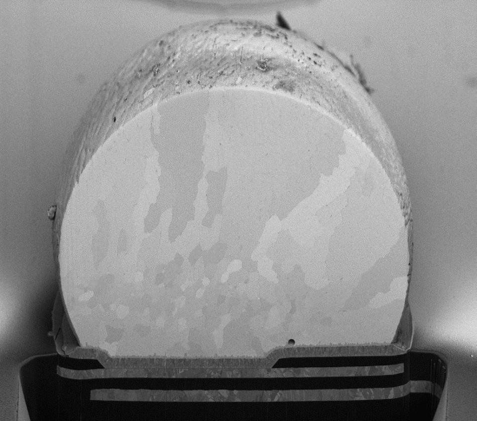
SEM image of solder ball cross-section taken at 2 keV using BSE detector showing excellent material contrast
Conventional Ga ion FIB sources have been limited to prepare small-area cross-sectioning not exceeding a couple of microns wide. Thus, typical failure analysis in packaging including solder balls combines cleaving and Ga FIB fine polishing for precise end-pointing to prepare cross-sections.
 Want to know more? Click here to read the full article
TESCAN Group
Founded in 1991 by a group of managers and engineers from Tesla with its electron microscopy history starting in the 1950’s, today TESCAN is a globally renowned supplier of Focused Ion Beam workstations, Scanning Electron Microscopes and Optical Microscopes. TESCAN’s innovative solutions and collaborative nature with its customers have won it a leading position in the world of nano- and microtechnology. The company is proud to participate in premier research projects with prominent institutions across a range of scientific fields. TESCAN provides its clients with leading-class products in terms of value, quality and reliability. TESCAN Group is the North American arm of TESCAN Group, a multinational company established by the merger of Czech company TESCAN, a leading global supplier of SEMs and Focused Ion Beam workstations, and the French company ORSAY PHYSICS, a world leader in customized Focused Ion Beam and Electron Beam technology.

This information has been sourced, reviewed and adapted from materials provided by TESCAN Group.
For more information on this source, please visit TESCAN Group.