Conventional Destructive Test Methods
The performance of today’ electronic products relies heavily on the integrity of the tiny connections between microchips and circuits, which can number as many as 2,200. These bonds are tested manually using bond pull and bond shear techniques, but their destructive nature means tests are carried out on representative samples rather than the actual product. By assuming the integrity of 50 products, when only five have been tested as good can have serious ramifications, particularly in the medical industry in which a defective bond in a pacemaker, for example, can lead to the death of a patient. It is these obvious weak spots that have inspired a team of researchers to revise the testing methods completely by developing a nondestructive system that uses light to test the integrity of bonds at least 30 times faster than the pulling and shearing methods.
An Alternative Non-Destructive testing Technique for Electronic Connections
As the demand for smaller, lighter and more reliable products increases, the space between the connections in microelectronics decreases. The micro laser ultrasonic bond detection system developed by Simpex Technologies and the Idaho Engineering and Environmental Laboratory (INEEL) in the USA, is a high-speed, non-contact, nondestructive method of determining the bond integrity of materials at the micro-level. The technology uses two tightly focussed light beams and can therefore test the integrity of bonds within nano-scale spaces of less than 0.0005 inches.
How Conventional Bond Integrity Test Techniques Work
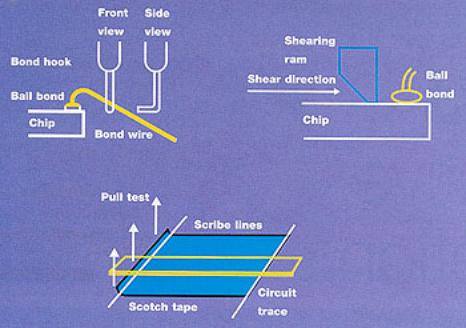
The current methods for bond integrity testing are the bond pull and bond shear methods, figure 1. As the name suggests, the bond pull technique requires the operator to use a small hook to snag each wire connection, giving them a controlled tug. If the bond stays attached, it gets a green light. In the bond shear test a ram is positioned against the base of the ball bond. The ram then pushes against the bond, ultimately breaking it off. The force required to break it free measures the bond’s strength. These methods are both time consuming and damaging to the interconnections, and are a far from perfect approach to testing electronic products given the sophistication of today’s semiconductor industry.
|
|
|
Figure 1. Schematic showing how current pull and shear bond test methods for testing of electronic products work.
|
How the Non-Destructive Bond Test Technique Works
The R&D 100 award winning invention uses an ultrasonic approach to bond detection by combining two different lasers - a pulse laser and a continuous wave laser detector. The concept behind the method is very similar to observing the waves from a pebble that has been thrown into a pond. The first laser sends multiple pulses of controlled light energy onto the top of the bond, generating thermal elastic propagations, or waves. Nearby, the second laser monitors the bonding surface. As the waves travel outwards through the neighbouring materials, the continuous wave laser detects and measures the wave patterns at a given location. This information is then fed into specialised computer software that assesses the wave’s characteristics. Using its extensive database of material responses, the Simpex technology can determine a good or bad bond. A strong ultrasonic signal indicates a strong bond, while no signal indicates a weak one.
Advantages of the Non-Destructive Test Technique
The system’s detection technique improves greatly on traditional contact type techniques. No direct contact is made with the object, the excitation is much gentler than that required in a contact test and the speed of testing is much faster than any automated assembly machine, allowing real-time process control.
Real Time Testing on Production Lines
Today’s automatic wire bonding machines can install 10 wires per second. However, Simpex’s technique can test each connection in just 200 nanoseconds. With such speed, a Simpex testing device could be incorporated into the manufacturing process to provide real-time, in-situ verification of bonds. ‘Today, they can’t test bonds fast enough to keep up with the bonding process,’ says Bernard Siu, President of Simpex Technologies and primary developer of the technology `With our approach, they might be able to catch up.’
Where the Technique can be Used
The bond detection system offers a non-contact test technique whenever optical access to the material’s surface is available, including locations with tight curvatures such as corners and edges. This fact allows its use in many processing environments in which contacting the material’s surface is not possible or desired. Using lasers for both the generation and detection of the elastic waves allows the technique to be used in environments in which the components that need to be examined are so fragile that contact sensing is inappropriate.
The Future for the Technique
Experts from the Johns Hopkins University of Applied Physics Laboratory and the National Institute of Standards and Technology have played an integral part in the creation of the detection system, primarily by testing the system during its development, which has taken four years. The system’s co-developers predict their new method will revamp the old testing standards, leading to more stringent tests of bond strength in today’s high-tech electronics that can be done in a fraction of the time. ‘With our bond detection system, industry will be able to test 100 percent of its products at the same cost or less than current methods without disturbing the form, fit or function of the product,’ says Siu.
Summary
Until now, the semiconductor industry has been left with no better way to determine the true bond quality of a product. Now, the micro laser ultrasonic bond detection system, not only offers a much better way to detect bonds, but offers the best of both worlds - it has the ability to help increase the quality of high performance electronics, including those used in weaponry, space and medical applications, while cutting the cost of production. Having built two prototype systems, the next challenge for Siu and his team is convincing the industry about the viability of this new test method - a task that could be easier than first thought based on the positive interest the system has received from industry so far.
|