Microelectromechanical systems (MEMS) are commonly used as actuators, sensors, radio frequency and microfluidic components throughout a variety of applications in health care, automotive and military industries. However, there are considerable challenges with both fabrication and packaging of such devices. In particular, issues related to yield and reliability need to be overcome.
Structures for motion sensors are generally composed of wafer-to-wafer (W2W) cavity die. The lid is bonded to the sensor with a metallic material (Fig. 1). Routine failure analysis consists of examining the bonding layer for manufacturing defects that may lead to malfunction. For this purpose, preparation of large-area cross sections at specific locations on the MEMS device is required. These cross sections are typically prepared by mechanical polishing, a technique which indeed enables large-area cross-sectioning but, on the other hand, induces severe artifacts such as delamination, tearing, mechanical stress or even the total destruction of a part of the die. Additionally, it is difficult to maintain control for end-pointing.
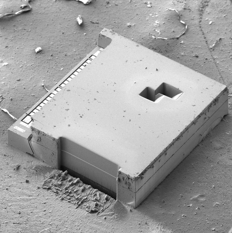
Fig. 1. MEMS with multiple cross-sections through the bonding layer of W2W cavity die.
TESCAN SOLARIS X is a Xe plasma Plasma FIB-SEM that provides an effective solution for preparing artifact-free, large-area cross-sections of MEMS for the purpose of device failure analysis. The great advantage of the Xe ion plasma FIB is its ability to generate a very high current ion beam while maintaining reasonable beam spot quality. This results in high sputtering rates, making it possible to remove large volumes of material in short timeframes. In combination with effective milling strategies, an artifactfree cross-section surface can be obtained. TESCAN SOLARIS X has everything necessary for preparing and analyzing large-cross-sections. The iFIB+™ Xe plasma FIB column, with unmatched field of view of 1 mm, is one of the essential features that enable the preparation of such large-area cross-sections. For imaging, the Triglav™ SEM column with immersion TriLens™ optics delivers excellent ultra-high-resolution performance, especially at low electron beam energies. Triglav™ also includes a unique in-beam detection system with BSE energy filtering and angular selective BSE detection. This improves materials contrast and enhances surface sensitivity, to enrich the information obtained during routine inspection of cross-sectioned MEMS.
 Want to know more? Click here to read the full article.
TESCAN Group
Founded in 1991 by a group of managers and engineers from Tesla with its electron microscopy history starting in the 1950’s, today TESCAN is a globally renowned supplier of Focused Ion Beam workstations, Scanning Electron Microscopes and Optical Microscopes. TESCAN’s innovative solutions and collaborative nature with its customers have won it a leading position in the world of nano- and microtechnology. The company is proud to participate in premier research projects with prominent institutions across a range of scientific fields. TESCAN provides its clients with leading-class products in terms of value, quality and reliability. TESCAN Group is the North American arm of TESCAN Group, a multinational company established by the merger of Czech company TESCAN, a leading global supplier of SEMs and Focused Ion Beam workstations, and the French company ORSAY PHYSICS, a world leader in customized Focused Ion Beam and Electron Beam technology.

This information has been sourced, reviewed and adapted from materials provided by TESCAN Group.
For more information on this source, please visit TESCAN Group.