The technique of Cathodoluminescence (CL) is commonly utilized in electron microscopy. It is regularly applied in a range of geological studies, which includes defect states and dating. Additionally, CL is used in materials science to offer information on the photonic properties of semiconductors, such as solar cells.
In addition to this, CL is used in pharmaceuticals to examine the distribution of active pharmaceutical ingredients. This article will explain how this type of CL work can be promptly and simply undertaken in Hitachi’s TM4000Plus benchtop SEM.
CL is one of an array of processes that may take place when an energetic electron beam impinges on a sample. More frequently, SEM’s use electron signals such as secondary electrons (SE) for topographical imaging, and backscatter electrons (BSE) for compositional imaging.
In addition to these electron signals, a spectrum of electromagnetic radiation is generated. This includes x-rays, which are used for elemental analysis (EDX/EDS). In certain materials, photons in the infrared, visible and UV wavelengths can also be emitted. These photons can contain valuable information about subtle compositional variations, bandgap, chemical bonding, crystal structure and defects.
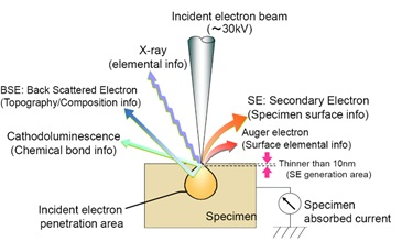
Figure 1. Typical interactions and signals in SEM. Image Credit: Hitachi High-Tech Europe
Conventionally, CL imaging is undertaken by adding a dedicated photon detector to an SEM. The detector gathers photons rather than electrons and may be panchromatic (identifying a wide range of wavelengths) or monochromatic (identifying specific wavelengths as required). Additionally, it may consist of a simple light guide and photomultiplier tube positioned towards the specimen.
In order to increase collection efficiency, the detector may also be comprised of a parabolic mirror directly above the specimen (which is connected to a photomultiplier tube or a spectrometer if spectral analysis of the photon wavelength is necessary).
The Hitachi TM4000Plus, however, provides the ability to identify panchromatic CL without any adjustment. This creates an opportunity to undertake a large number of panchromatic CL investigations simply and effectively in a cost-effective, readily available instrument.
The TM4000Plus contains a low vacuum secondary electron detector (referred to as UVD) based on light collection technology, meaning CL detection may be accomplished simply by the touch of a button. The bias which is typically applied to enhance secondary electron detection is switched off, meaning the detector functions as a photon detector, with the secondary electron signal suppressed.
As the TM40000Plus also contains a high-performance backscatter electron detector and dual-channel image handling capability, it is possible to obtain compositional and CL information concurrently ( shown in the example in Fig 2. below). The datasets can be stronger if the (optional) EDX elemental mapping capability is utilized, meaning qualitative and quantitative chemical information can be provided promptly.
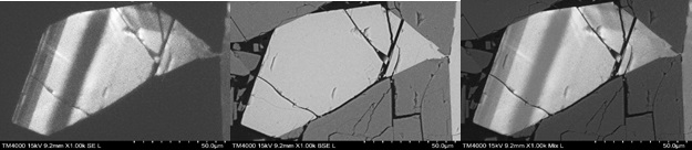
Figure 2. Zonation study in coarse grained syenite with alkali feldspar From left – CL image showing zonation, BSE image showing composition contrast and Mixed (CL + BSE) image recorded simultaneously. Image Credit: Hitachi High-Tech Europe
CL Imaging of Materials Science
In materials science, CL imaging is a formidable technique to aid understanding of the crystallographic properties or bonding state of materials. In the example below, a multi-phase TiO2 sample was examined. No substantial contrast variation is detected in the backscatter electron image (left) due to the lack of compositional variation across the specimen.
However, in the CL image (right), distinct regions are evident. These relate to the rutile and anatase phase of TiO2. Since the CL detector in the TM4000Plus is more sensitive in the shorter wavelength range, the anatase phase appears bright, whereas the rutile phase (where emitted photons have a wavelength >500 nm) looks dark.
Using this prompt and straightforward method avoids the necessity to undertake separate spectrophotometry or diffraction studies and provides spatially resolved information at the sub-µm scale, which is not easy to attain from other techniques.
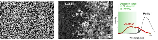
Image Credit: Hitachi High-Tech Europe
CL Imaging in Pharmaceuticals
In a pharmaceutical drug delivery system like a simple tablet, the correct distribution of the Active Pharmaceutical Ingredient (API) is crucial. The particle size and distribution of the API must be meticulously controlled to guarantee efficient uptake in the body. Below is an example of a cross-section through a commercial ibuprofen tablet.
The secondary electron image (left) shows the roughness associated with the fracture of the tablet. The backscatter electron image (center) displays the enteric (gastric resistant) coating encompassing the tablet itself. The CL image (right), however, shows comprehensive information about the distribution of the API. This information may be used for both rapid process control and quality control.
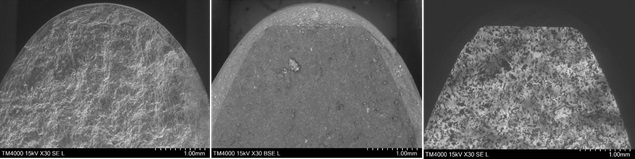
Image Credit: Hitachi High-Tech Europe
CL Imaging in Geology
CL is broadly used in geology to examine subtle variations in how the crystals are formed which is less likely to be noticeable from secondary electron imaging, backscatter electron imaging or energy-dispersive X-ray analysis. In the syenite example below, due to their being little or no compositional change, the BSE image (middle) displays no brightness variation across the crystal. The CL image, however, displays strong brightness variation across the crystal due to zonation.
A further example of a process where the technique may be readily applied is to support geological dating of zircons. Variations in U-Th-Pb ratios within zircon crystals may be used to ascertain the date of formation of the crystal. The minor variation in U-Th-Pb ratio is smaller than can be reliably identified with chemical techniques in the SEM such as EDX. The exact ratio of the elements is determined precisely by mass spectrometry instead. However, the mass spectrometer cannot quickly identify areas of interest to examine, which presents a challenge.
As such, in SEM, CL can play a powerful role in determining areas of interest for further analysis and can considerably speed up the dating process. The “zoning” evident in CL images of zircons gives an indication of which grains exhibit the biggest variations in U-Th-Pb ratios, guides the geologist to undertake mass spectrometry on the most suitable crystals.
In the example of Fig. 3 below, a zircon imaged in conventional SEM with the dedicated CL detector (right) is compared with CL imaging of the same crystal in TM4000Plus (left). Comparable information is evident and both approaches offer the information necessary to select the best possible grains for subsequent mass spectrometry.
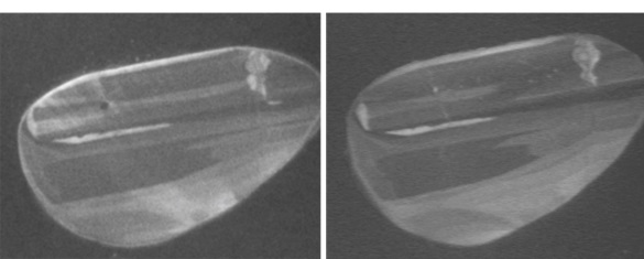
Figure 3. Zircon grains imaged using the Hitachi TM4000Plus (left) and pan-chromatic CL detector in conventional SEM (right). Image Credit: Hitachi High-Tech Europe
Conclusion
Panchromatic imaging capability can be successfully performed in a Hitachi benchtop SEM to aid the understanding of a broad range of materials systems. The capability to overlay BSE and CL data in one image presents users with precise correlation of chemical and crystallographic or bonding information –be it as standalone studies or to support additional investigations such as subsequent spectrometry or diffraction studies.
These instruments need a smaller amount of capital investment and lab space, they offer quicker time-to-data and can be used without much difficulty by any operator regardless of previous electron microscope experience. This means that they present the opportunity for CL studies to be applied far more broadly than previously. This enables the power of CL to be accessible in many more labs than in the past, including for process and quality control as well as in academic environments.
In addition to this, the Hitachi benchtop SEMs offer the capacity to undertake this type of CL work without any adjustment or any additional hardware investment. Combined with secondary electron (SE) and backscatter electron (BSE) imaging, in addition to EDX elemental analysis and mapping, this kind of instrument provides a powerful addition to pharmaceutical labs, geoscience labs and a broad range of materials science labs.
Equipment Used
Hitachi TM4000Plus benchtop SEM in standard configuration.
Image Credit: Hitachi High-Tech Europe
Acknowledgments:
Many thanks to Dr. Eszter Badenszki, University College Dublin, School of Earth Sciences, for providing the Zircons and CL Images for inclusion in this study
Many thanks to Dr. Adam Jeffery, School of Geography, Geology and the Environment, Keele University for the Syenite sample

This information has been sourced, reviewed and adapted from materials provided by Hitachi High-Tech Europe.
For more information on this source, please visit Hitachi High-Tech Europe.