Nanomaterials can be described as materials that possess a nanoscale dimension that is between 1 and 100 nm. Using nanotechnology in order to create nanomaterials for various applications has been a useful part of evolving different industries from semiconductors to creating innovative devices.
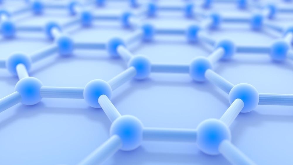
Image Credit: James A Isbell/Shutterstock.com
Utilizing top-down nanostructuring of two-dimensional (2D) materials results in nanomaterials that have specific electrical and optical properties through a quick and flexible method. However, two-dimensional materials are liable to contamination and edge disorder, and so in order to rectify these challenges, various techniques have been explored such as scanning probe lithography, or direct beam lithography. This article will explore a novel method that has the potential to design nanomaterials with less than 10 nm precision.
A research collaboration between the Technical University of Denmark (DTU) and the Graphene Flagship has included innovative development consisting of patterning nanomaterials with a higher level of precision.
The precise patterning of 2D materials is significant for advanced computation and storage which can be innovated in order for higher performance without the increased power consumption that is required currently. The advancement of patterning 2D materials has consisted of the researchers at DTU using sophisticated lithography machines which utilized nanostructured graphene. The research was supported by The Graphene Flagship.
Graphene
With the discovery of graphene, a carbon allotrope that is four times stronger than steel, light-weight, and has excellent thermal and electrical conductance, the application of this novel material was endless.
The ability to program and modify graphene and create delicate patterns made it a desirable material, and by altering its properties to increase suitability for critical applications, it was the perfect model for precision control.
The researchers have advanced current lithography technology with an electron beam lithography system that can go below 10 nanometers. They analyzed how dry anisotropic etching of multilayer 2D materials with sulfur hexafluoride can overcome challenges associated with top-down lithography processes which can affect the efficacy in performance of 2D materials.
Lene Gammelgaard, a research engineering graduate working in DTU, explained,
"The trick is to place the nanomaterial hexagonal boron-nitride on top of the material you want to pattern. Then you drill holes with a particular etching recipe.”
He continued that, "The etching process we developed over the past years down-size patterns below our electron beam lithography systems' otherwise unbreakable limit of approximately 10 nanometers. Suppose we make a circular hole with a diameter of 20 nanometers; the hole in the graphene can then be downsized to 10 nanometers.
While if we make a triangular hole, with the round holes coming from the lithography system, the downsizing will make a smaller triangle with self-sharpened corners. Usually, patterns get more imperfect when you make them smaller. This is the opposite, and this allows us to recreate the structures the theoretical predictions tell us are optimal."
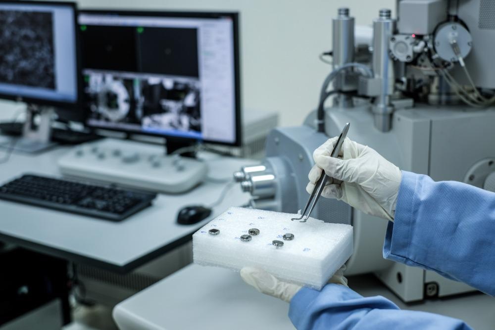
Image Credit: Anucha Cheechang/Shutterstock.com
Benefits of The Novel Method
Using this innovation, computer calculations have the ability to predict the shape and size of patterns within graphene to a higher precision level. This can be used for a variety of applications and advance different industries such as electronics and semiconductors. By being able to alter electron and quantum properties, this can result in higher efficiency associated with calculations with high speed without consuming as much power or energy.
The challenge behind this aim would be the optimization that would require a higher resolution of the atomic level, which is a challenge for conventional lithography systems.
However, in undergoing this research of reaching an atomic resolution, these scientists have been able to overcome this obstacle.
Previously, they were able to illustrate that circular holes which are placed 12 nm apart resulted in turning the semi-metallic graphene material into a semiconductor, and with their advancement in creating circular holes and triangles with nanometer sharp corners, other patterns have been experimented with. These types of patterns are able to sort electrons based on their spin and create critical components for valleytronics and other applications. With this concept working on 2D materials, it can enable more technologically advanced communication as well as innovative biotechnology.
Innovative Applications
The research undertaken by these innovative material scientists has revolutionized the patterning of 2D materials with anisotropic dry etching, which led to very well-defined hexagonal structures as well as enabling the definition of features under 10 nm. However, to increase this level and utilize the nanoscale further would require further research, but with this novel advancement, anisotropic dry etching can aid the development of various industries with promising outlooks for creating high-performing devices.
The novel design method can enable the researchers to produce flat electronic meta-lenses, which are a type of highly compact optical lens that can be controlled electrically at high frequencies. This may revolutionize telecommunications and advance technology into a more innovative future.
Further Reading and References
Danielsen, D., Lyksborg-Andersen, A., Nielsen, K., Jessen, B., Booth, T., Doan, M., Zhou, Y., Bøggild, P. and Gammelgaard, L., 2021. Super-Resolution Nanolithography of Two-Dimensional Materials by Anisotropic Etching. ACS Applied Materials & Interfaces, 13(35), pp.41886-41894.
DOI: https://doi.org/10.1021/acsami.1c09923
Science Daily. 2021. Quantum materials cut closer than ever. [online] Available at: <https://www.sciencedaily.com/releases/2021/09/210913135701.htm> [Accessed 21 October 2021].
Disclaimer: The views expressed here are those of the author expressed in their private capacity and do not necessarily represent the views of AZoM.com Limited T/A AZoNetwork the owner and operator of this website. This disclaimer forms part of the Terms and conditions of use of this website.