This article presents an overview of the semiconductor manufacturing process, with a particular focus on the use of etching technology, as well as the latest research that is happening in this field.
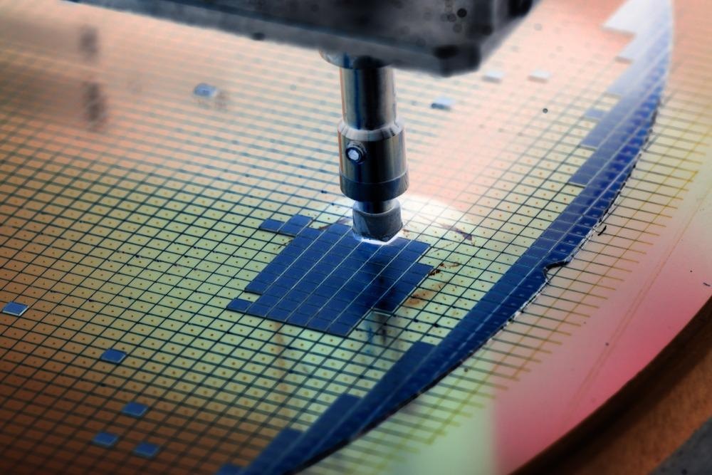
Image Credit: Macro photo/Shutterstock.com
Semiconductors: The Brain of Modern Electronics
Semiconductors are a crucial element of electronic equipment, allowing for advancements in telecommunications, computers, biotechnology, weapons technology, aviation, renewable energy, and a variety of other fields. Semiconductors, also known as integrated circuits (ICs) or microchips, are produced from pure substances such as silicon and germanium, as well as composites like gallium arsenide.
Small quantities of defects are introduced to these pristine components in a process called doping, producing dramatic variations in the conduction of the material. Smartphones, electronic goods, communication devices, automation systems, automotive parts, and military infrastructure all use semiconductors. These products include semiconductor materials that perform cognitive control, imaging, power management, storage solutions, signal conditioning, and conversion between optical and electronic sources of power.
A Brief Overview of the Semiconductor Manufacturing Process
The semiconductor manufacturing technique is composed of multiple distinct production steps, each of which results in a specific range of processes. Numerous tiny circuits are created on the wafer using a variety of physical and chemical processes. The process begins with the use of a silicon wafer platform. Wafers are formed from a salami-shaped strip of virtually pure silicon (ingot) that has been polished to perfection. Silicon dioxide is manufactured or deposited on the wafer to act as a protective coating or protection.
Following that, a light-sensitive layer called a photoresist is applied to the wafer. The two types of resistance are positive and negative. Photolithography is a critical stage since it determines the arrangement of transistors on the chip. At this stage, the chip wafer is placed in lithographic equipment and exposed to deep ultraviolet (DUV) or extreme ultraviolet (EUV) radiation. Unwanted areas of the silicon structure are removed to expose a basic material or to allow for the coating of an additional component rather than the etched coating. Conducting metal is deposited onto the wafer to produce the microchip's conduction areas. Finally, the excess material is removed from the wafer's bottom, resulting in a nice, smooth finish.
Semiconductor Etching Technology and its Types
In the manufacturing of semiconductor devices, etching corresponds to any technique that removes material systematically from a thin layer on a platform (with or without preceding architecture on its interface) and leaves behind a sequence of that substance on the platform. A cover that is resistive to the etch defines the layout. Once the cover is in position, the exposed material may be etched using either "wet (chemical)" or "dry (physical)" processes.
Traditionally, wet chemical processes were critical in a pattern defining etch. However, as system component dimensions shrank and the importance of interface topographies increased, wet chemical etching was displaced by dry etching methods. This change was principally caused by wet etching's isotropic composition.
More from AZoM: Lithography Machines and the Chip-Making Process
Wet etching removes material in all dimensions, resulting in a difference in the size of the structures specified by the covering and those duplicated on the platform. Dry etching may be used to remove material by physical techniques such as ion impact followed by material expulsion from the surface or chemical processes that convert the surface to gaseous reactive species that can be blown away. All dry etching processes operate in a vacuum, with pressure determining the character of the etch phenomena to some degree.
Plasma etching is another significant etching method. Plasma etching procedures take advantage of the molecular and atomic charges and/or reacting neutrals contained in plasma to remove material from the surface. Purely physical etching is performed by accelerating positive atomic charges toward the surface using intense electrical currents. When the ions collide with the surface layer, their intrinsic power is transported to the substrate's molecules. A substrate molecule will be expelled into the gaseous state and sucked away by the vacuum pump if sufficient energy is delivered.
The Latest Research
A recent study published in the journal ACS Omega by a group of Italian researchers discusses the development and characterization of trenches on the Silicon Carbide (SiC) classification surface through plasma etching with SF6. The researchers monitored and accurately controlled the trench depth using interferometric endpoint detection (IEPD).
Transmission electron microscopy and X-ray photoemission spectrometer studies demonstrated that the trenches created are of good quality and uniformity. Due to plasma etching with O2 and SF6, it was revealed that SiC surface modification was very minor, with no indication of fluoride poisoning. These results demonstrate that the trenches created by plasma etching on the SiC platform are well suited for fabricating next-generation electronic devices.
In short, many advances are being made in the field of semiconductor etching technology, paving the way for future applications.
References and Further Reading
ASML, 2022. 6 Crucial steps in semiconductor manufacturing. [Online]
Available at: https://www.asml.com/en/news/stories/2021/semiconductor-manufacturing-process-steps
[Accessed 6 March 2022].
MKS Instruements, 2022. Semiconductor Etching. [Online]
Available at: https://www.mks.com/.
[Accessed 22 March 2022].
Pirnaci, Massimo D., et al. 2021. Systematic Characterization of Plasma-Etched Trenches on 4H-SiC Wafers. ACS Omega. 6(31). 20667-20675. Available at: https://pubs.acs.org/doi/10.1021/acsomega.1c02905
Racka-Szmidt, Katarzyna, et al. 2021. A Review: Inductively Coupled Plasma Reactive Ion Etching of Silicon Carbide. Materials 15(1). 123. Available at: https://www.mdpi.com/1996-1944/15/1/123
Guo, Haoming, et al. 2022. A review on the mainstream through-silicon via etching methods. Materials Science in Semiconductor Processing 137. 106182. Available at: https://www.sciencedirect.com/science/article/pii/S1369800121005205?via%3Dihub
Disclaimer: The views expressed here are those of the author expressed in their private capacity and do not necessarily represent the views of AZoM.com Limited T/A AZoNetwork the owner and operator of this website. This disclaimer forms part of the Terms and conditions of use of this website.