Six critical steps are involved in the manufacturing of semiconductors. These steps include deposition, photoresist, lithography, etch, ionization and packaging. This article discusses several ionization processes.
What is the Ionization Process?
The process of formation of ions from an atom or a molecule either by the gain or loss of electrons is known as ionization. There may be a loss or gain of energy during the ionization process. An anion is a negatively charged ion that is formed by the gain of electrons by an atom or a molecule. Similarly, a positively charged ion formed by the loss of electrons from an atom or a molecule is called a cation.
Ionization is also called ion implantation, which means the process of modification of a material’s surface by which ions of one material are implanted to another, which causes a change in physical and chemical properties.
What are Semiconductors?
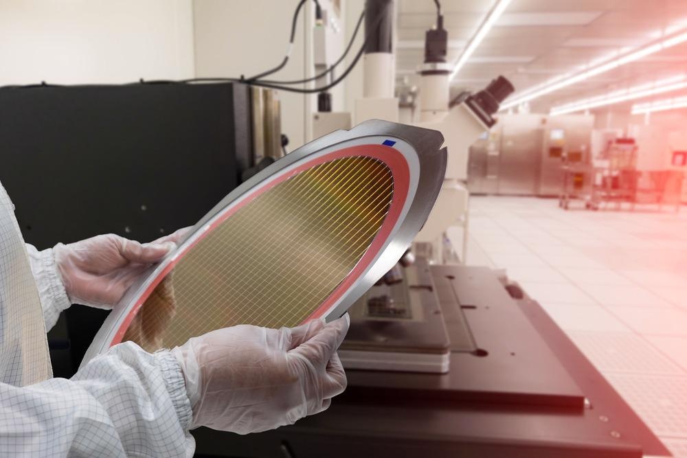
Semiconductors can be compounds like cadmium selenide, gallium arsenide, or elements such as germanium or silicon. Semiconductors are used in the fabrication of many kinds of electronic devices such as ICs, transistors, and diodes. These electronic devices have a wide range of applications because of their low cost, power efficiency, reliability, and compactness.
Ionization in Manufacturing of Semiconductors
Ion implantation is applied to semiconductors to control concentrations of p-type and n-type dopants at an accurate distance from the surface. It is a very crucial process for the fabrication of ICs. While fabricating semiconductors, the ion implantation process comes into play after deposition, photoresist, lithography, and etching.
Ionization is used to tune conducting properties of part of the pattern. After the etching of silicon wafers, these are bombarded with negative and positive ions. Silicon inherently is neither a perfect insulator nor a conductor, since its properties are in-between.
Transistors are building blocks for any microchip. Transistors are created by bombarding electrically charged ions on silicon crystals, allowing a controlled electricity flow. After ionization of the required layer, the resists are removed. The resists are usually placed for the protection of an area that does not need etching or ionization.
Ion Implantation Equipment
Ionization equipment has several parts, including a target chamber, an accelerator (accelerating ions at high energy), and an ion source of the chosen element. Conventionally, ions are removed from the source, the accelerator excites them to high energy, and then these high energy ions are bombarded to the workpiece. This process is known as conventional beam-line ion implantation. In this process the ion beam is small; therefore, to get uniform implantation over a large area, the ion beam or sample is raster scanned. However, this method is not very effective for complicated geometries since it is challenging to achieve conformal ion implantation.
Fast Neutron Irradiation vs Irradiation through Ion Implantation
The damaged pattern is produced by low-temperature irradiation of semiconductors with fast neutrons. The bombarded neutrons collide with lattice atoms causing the ejection of some atoms from the lattice site. With this process, sufficient energy is received for the initiation of a cascade of more knock-ons. Therefore a region is generated that contains high vacancies. This region is known as the depleted or diluted region.
The depleted region is surrounded by these kicked-out atoms acting as interstitial atoms. This separation between the deleted and interstitial region is sometimes very large, up to 100-times the atomic distance, since these are transported away through replacement chains propagating with low energy dissipation.
Irradiation with ion implantation is done with the help of protons or alpha particles. It causes damage to patterns ranging from homogeneous distribution of point defects as obtained after electron irradiation, to heavily damaged regions that are characteristic of fast neutron irradiation. The nature of this damage is dependent on irradiation temperature, energy and dose, ion species, and the structure of irradiated material and its chemical composition.
Plasma Immersion Ion Implantation
Plasma immersion ion implantation, or PIII, is an advanced technique that is used for ionization during the manufacturing of semiconductors since it can process complex-shaped samples more conveniently. The specimen in this process is encircled by plasma and pulse-biased to high negative potential compared to the chamber wall. A plasma cover is therefore generated around the specimen. Ions are then accelerated across this plasma covering and are implanted into the surface. The plasma is created in the vacuum chamber through several plasma sources like radio frequency (RF) or electron cyclotron resonance (ECR).
Applications of Ionization of Semiconductors
Ion implantation is used for forming conducting layers as well as insulating compounds in semiconductor devices. Several technological issues like reducing TED dopants and removal of metals from active regions of the device have been solved by the introduction of ionization processes. Controlled ion damage is of critical importance for improving semiconductor devices' performance and altering device properties as per requirements.
More from AZoM: Digitizing the Process Industry
References and Further Reading
Crowder, B. (Ed.). (2013). Ion implantation in semiconductors and other materials. Springer Science & Business Media. https://books.google.com.pk/books?hl=en&lr=&id=c_kICAAAQBAJ&oi=fnd&pg=PA3&dq=+Ion+Implantation+in+Semiconductors+and+Other+Materials&ots=NeO1CrtMPY&sig=o8QUI3mSFebFlKp4aU4tmNyxbMw&redir_esc=y#v=onepage&q=Ion%20Implantation%20in%20Semiconductors%20and%20Other%20Materials&f=false
Timings, J., 2021. 6 crucial steps in semiconductor manufacturing. [online] Asml.com. Available at: <https://www.asml.com/en/news/stories/2021/semiconductor-manufacturing-process-steps#:~:text=To%20make%20any%20chip%2C%20numerous,%2C%20etch%2C%20ionization%20and%20packaging
Williams, J. S. (1998). Ion implantation of semiconductors. Materials Science and Engineering: A, 253(1-2), 8-15. https://www.researchgate.net/publication/258937256
Disclaimer: The views expressed here are those of the author expressed in their private capacity and do not necessarily represent the views of AZoM.com Limited T/A AZoNetwork the owner and operator of this website. This disclaimer forms part of the Terms and conditions of use of this website.