Auger Electron Spectroscopy (AES) is a popular analytical technique utilized extensively in materials science and microelectronics, especially in the semiconductor industry. This article looks at the basics of Auger Electron microscopy, its advantages, limitations, and its utilization in the semiconductor industry.
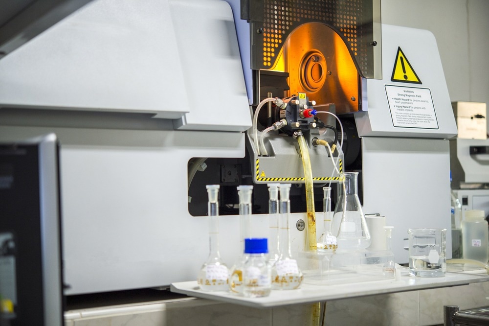
Image Credit: Rabbitmindphoto/Shutterstock.com
What is Auger Electron Spectroscopy (AES)?
Analyzing the features of various types of substrates involves the application of the essential analytical technique known as Auger Electron Spectroscopy (AES). It can generate surface images of several kinds of conductive and semiconducting materials and gather information on the layer thickness and chemical compositions of those materials.
Uses of AES
AES has been used to explore a wide range of surface-mediated processes, including the generation of slender films and coatings on substrates as well as adsorption, catalytic reactions, oxidation/reduction, photochemical, and dissolution/precipitation reactions. All elements can be detected by AES, except H and He.
Auger Effect – The Working Principle of AES
AES is a method that makes use of the Auger effect to discover crucial details about the interfaces of diverse materials. The removal of an electron from an orbit of lower orbital energy typically by a collision with another electron results in the occurrence of the Auger effect. As a result, there is a vacancy that will eventually be filled by an electron from an orbit with higher energy.
A secondary electron will transmit the surplus energy by using it as kinetic energy to gain freedom from the atom while still being expelled in the meantime. An Auger electron is the kind of electron that emerges from an atom in this manner.
An Auger electron possesses a very precise amount of momentum/kinetic energy when it is released. An accurate analysis of the energy carried by the electrons is essential to obtain data about elemental configuration and present an image of the surface.
Advantages of Auger Electron Spectroscopy
This is a highly sensitive spectroscopic technique with accurate detection capabilities even for the nanoscale region. The elemental analysis of all elements with atomic mass greater than 3 could accurately be performed. At a sub-micron resolution, mapping of the abundance of components on the substrate surface can be generated. This is highly helpful for figuring out if the interfaces of materials are homogeneous or heterogeneous in terms of composition.
The densities of outer layers on a substrate platform could also be determined using depth profiling patterns obtained from an ion sputter gun. Monitoring variations in physio-chemical conditions placed on substances relies heavily on the capacity to collect molecular stratigraphic data at the nanometer scale.
Furthermore, documented Auger sensitivity factors may be used to create semi-quantitative assessments, or standards could be compared.
Limitations of Auger Electron Spectroscopy
Among the various advantages AES offers, several limitations need to be addressed.
AES can only analyze conducting materials and semiconductors because they can rapidly transmit electrons across the material. This is because AES relies on the utilization of an energetic electron beam to investigate surfaces. As a result, it is typically not appropriate for assessing insulating materials.
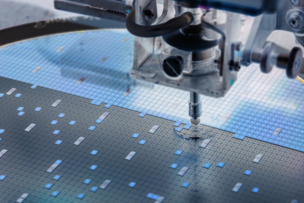
Image Credit: Macro photo/Shutterstock.com
Material interface pollution is virtually always prevalent, necessitating some preparatory coating ablation. Materials must be suitable for an environment with an ultrahigh vacuum. Due to potentially harmful effects, materials that are flammable or flammable under an electron beam should not be studied.
Instrumentation for AES Analysis
An AES equipment is essentially an enhanced SEM that additionally has an ion sputter gun, an Auger electron detector, and an ultrahigh vacuum chamber.
Standard pictures are produced by AES by stimulating the surface layer with a focused electron beam. For specialized AES investigations, these images offer contour plots of the components or textures that can be used to define objects of interest. Field emission electron sources are commonly used in modern AES devices, enabling spatial resolution of fewer than 5 nanometers.
In order to remove superficial impurities, the ion blaster also directs a focused pulse of an ionized gas (often Argon) at the sample. Any adsorbent vapors will be identified on a semiconductor "as received" that have been in touch with the surroundings since the AES originates from just a few atomic monolayers at the surface of the material.
Use in the Semiconductor Industry
To gather the necessary data, the semiconductor sector is dependent on the powerful mix of AES and the sputter etching procedure.
AES has made a significant contribution to the field of very-large-scale integration (VLSI) technology, which involves ion implanting high dopant quantities into devices with minimal layer depths. The high dopant concentration level used in VLSI frameworks has created an opportunity for AES to complement ion mass spectroscopy (SIMS) analysis.
Contact interaction is yet another situation where Auger characterization is particularly useful. The Schottky barrier connection, which forms a barrier potential and possesses resolving qualities akin to a p-n junction, is a connection between a metal and a semiconductor. Numerous AES investigations have focused on chemical reactions at the metal-semiconductor interface, which determines how barriers arise.
Latest Research
As per the latest research published in Applied Sciences, a novel and efficient fabrication technique for semiconductor manufacturing are essential. Highly uniform (FDTS) SAM films were manufactured and analyzed using AES to determine their efficiency. Three areas comprising two dark regions and a solitary light region were selected for analysis.
At 648 eV, noticeable fluoride KLL Auger particles (F1) were found in the two dark regions. O1 and O2 KLL Auger electrons for the oxygen elements were found at 479 eV and 502 eV, respectively. Fluorine KLL Auger electron concentrations were substantially higher in Areas 1 and 3 (11.7% and 10.3%, respectively), which had FDTS SAM patterns, than they were in Area 2 (0.36%), which contained silicon dioxide structures.
The analysis results showed that FDTS SAM film designs based on the vapor coating methods are extremely consistent with the FDTS SAM film patterns created using chip manufacturing processes.
In short, it is safe to say that the utilization of AES for metrological techniques in the semiconductor industry is highly beneficial for industry-scale state-of-the-art nanoscale fabrication.
More from AZoM: Latest Advancements in MOF Use in Semiconductor Devices
References and Further Reading
Measurlabs, 2022. Auger electron spectroscopy (AES)q. [Online] Available at: https://measurlabs.com/methods/auger-electron-spectroscopy-aes/
Li S et. al. (2022). Auger Electron Spectroscopy (AES) and X-ray Photoelectron Spectroscopy (XPS) Profiling of Self Assembled Monolayer (SAM) Patterns Based on Vapor Deposition Technique. Applied Sciences. 12(3). 1245. Available at: https://doi.org/10.3390/app12031245
Mogk, D., 2022. Auger Electron Spectroscopy. [Online] Available at: https://serc.carleton.edu/msu_nanotech/methods/aes.html
Shekhter, D. P., 2022. Auger Electron Spectroscopy (AES) and X-ray Photoelectron Spectroscopy (XPS) Laboratory. [Online]
Available at: https://en-wolfson.tau.ac.il/laboratories/auger-electron-spectroscopy-aes-and-x-ray-photoelectron-spectroscopy-xps-laboratory
Atzrodt, V., & Lange, H. (2022). Principal component analysis as a method for silicide investigation with Auger electron spectroscopy. 79(2). 489-497. Available at: https://doi.org/10.1515/9783112500965-02
Disclaimer: The views expressed here are those of the author expressed in their private capacity and do not necessarily represent the views of AZoM.com Limited T/A AZoNetwork the owner and operator of this website. This disclaimer forms part of the Terms and conditions of use of this website.