Current research is focused on enhancing the electrical conductivity of MOFs, including mean charge transport either through space or through bonds, along with the fabrication of semiconductor devices and high-quality molecular thin films.
Image Credit: Phonlamai Photo/Shutterstock.com
What Are MOFs and Their Applications?
Metal-organic frameworks (MOFs) are a type of nano-porous, hybrid crystalline material consisting of either clusters with organic linkers or discrete metal ions. They are composed of multitopic ligands (arms) and metal-ion clusters (nodes). Discovered in 1995 by Prof. Yaghi and his team, MOFs are commonly prepared by the solvothermal method at high temperatures, with subsequent slow cooling. The arms and nodes form well-ordered, crystalline cage-like MOFs by coordinating with each other.
Due to their crystal engineering, MOFs can be exploited to coordinate their bonds into forming one, two, and three-dimensional networks (1D, 2D, 3D). 3D MOFs are promising due to their greater physical properties, as well as a longer pore diameter suitable for gas adsorption, small molecule storage, catalytic transformations, bio-medical applications, and photo-switching. Thin-film MOFs can also introduce defect densities in a contained manner during film formation.
However, MOFs offer disappointing electrical conductivity because of weak d-p orbital interactions between organic linkers and transition metal ions, despite their ease of preparation, high crystallinity, and inexpensive preparation. This makes them insufficient for microelectronic applications.
Recent Advancements of MFOs in Semiconductor Devices
Surface-mounted metal-organic frameworks (SURMOFs) are fabricated from bulk MOFs and are crystalline, thin, highly ordered structures of MOF films prepared either by drop-casting or spin coating onto various substrates. Among many synthetic approaches, liquid-phase epitaxy (LPE) can enable the formation of a hetero multilayer while providing well-defined contacts, thus influencing semiconductor device performances.
Additionally, the electrochemical deposition (ECD) technique is another method for designing MOF thin films and involves (1) anodic deposition, (2) cathodic deposition, and (3) electrophoretic deposition. The primary advantage of this method is that no dispersing agent or surfactant is involved. Heinke and co-workers established well-defined semiconducting using layer-by-layer (LbL) deposition of MOF films, thus giving a push to produce MOFs with improved electrical conductivity, charge separation efficiency, charge carrier mobility, and interface stability in semiconductor devices.
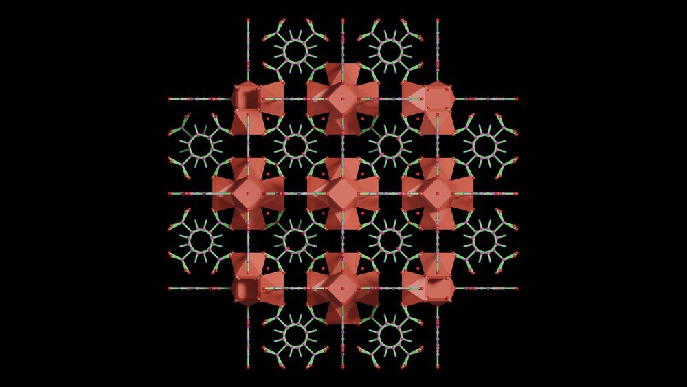
Image Credit: sanjaya viraj bandara/Shutterstock.com
Presently, MOFs are regarded as versatile electroactive materials, whose conductivity can be substantially improved by various measures. The conductivity of MOFs can be measured on polycrystalline and single-crystal samples in the form of thin pellets or films. Recently, it was reported that high conducting MOFs have conductivities similar to that of contact and wire. An electrical Li-ion intercalated MOF prepared by Rambabu et al exhibited a million-fold increment in electrical conductivity.
Furthermore, external stimuli such as magnetic or electric field, temperature, and light have played a crucial role in the moderation of the electric properties of MOFs. McGrail and co-workers reported that a MOF made up of Cu+2 metal node, and 7,7,8,8-tetracyanoqunidodimethane (TCNQ) linker could change the shape into either an insulating phase or a conducting phase when a potential is applied. A solvent can change the MOFs’ electronic properties as well, by modifying the geometry, chemical composition, or host-guest interactions.
Post-synthesis doping by exploiting the porosity of the MOFs has also resulted in exceptional amplification of charge transmission; e.g., embedding conducting polymer fibers or tuning of the band gap exhibited a drastic rise in conductivity.
2D and 3D MOFs
2D MOFs have been successful in real-world applications even though their charge transport mechanism is less understood. Recently, Day et al. observed that MOFs function as a metal at exceedingly low temperatures, while at high temperatures, they behave like semiconductors.
The preparation of 3D MOFs is challenging because of their high porosity. Hence, only a few such MOFs have been accounted for to date. However, Medina and co-workers recently described a microporous 3D conducting MOF comprising 2,3,6,7,10,11-hexahydroxytriphenylene (HHTP) linker and Fe (iii) metal node with a porosity of 1400m2/g.
Conclusions
To summarize, advances made in the development of MOF thin films can largely benefit semiconductor device applications. Recent years have seen an exponential increase in the thin-film MOFs’ surface-related chemical processes, thus facilitating a number of applications.
However, the control of crystallinity, morphology, roughness, conductivity, and film orientations in the devices remains a challenge. It is difficult to retain the bulk properties while simultaneously controlling the MOF particle orientation under an external electric field. The enhancements of the conductivity of MOF-based materials demand an understanding of the underlying solid-state physics. The intriguing complex structures that make up the MOFs impart multiple physical, chemical, optoelectronic, and electronic properties, which can be combined for further technological applications.
References and Further Reading
Ranjeev Kumar Parashar, Priyajit Jash, Prakash Chandra Mondal, Metal-Organic Frameworks in Semiconductor Devices: Recent Advancements and a Bright Future Materials Science, https://doi.org/10.48550/arXiv.2206.13473
Heinke, L., Wöll, C., Adv. Mater. 2019, 31, 1806324. https://doi.org/10.1002/adma.201806324
D. Rambabu, A.E. Lakraychi, J. Wang, L. Sieuw, D. Gupta, P. Apostol, G. Chanteux, T. Goossens, K. Robeyns, A. Vlad, J. Am. Chem. Soc. 143 (2021) 11641–11650. https://pubs.acs.org/doi/full/10.1021/jacs.1c04591
R.W. Day, D.K. Bediako, M. Rezaee, L.R. Parent, G. Skorupskii, M.Q. Arguilla, C.H. Hendon, I. Stassen, N.C. Gianneschi, P. Kim, M. Dincă, ACS Cent. Sci. 5 (2019) 1959–1964. https://pubs.acs.org/doi/full/10.1021/acscentsci.9b01006
C.A. Fernandez, P.C. Martin, T. Schaef, M.E. Bowden, P.K. Thallapally, L. Dang, W. Xu, X. Chen, B.P. McGrail, Sci. Rep. 4 (2015) 6114 https://opg.optica.org/oe/fulltext.cfm?uri=oe-23-11-13725&id=318843
A. Mähringer, et al. Angew. Chemie Int. Ed. 60 (2021) 18065–18072. https://onlinelibrary.wiley.com/doi/full/10.1002/anie.202102670
Disclaimer: The views expressed here are those of the author expressed in their private capacity and do not necessarily represent the views of AZoM.com Limited T/A AZoNetwork the owner and operator of this website. This disclaimer forms part of the Terms and conditions of use of this website.