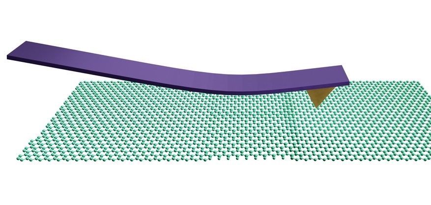
Atomic force microscopes (AFM) are a type of scanning probe microscope (SPM) used a probe to evaluate local characteristics such as friction, magnetism, and height. AFM acquires an image by raster-scanning the probe across a small sample area, while simultaneously assessing the local properties. This method can be used to assess thin films and coatings.

Image Credit: sanjaya viraj bandara/Shutterstock.com
Applications of AFM
AFM facilitates atomic resolution imaging of insulator and conductor surfaces. One of the techniques utilizing AFM is frequency-modulation AFM (FM-AFM), which has been used for the atomic-resolution imaging of Si, KCl, metal oxides, organic monolayers, as well as a physisorbed xenon film on graphite in the past decades. Additionally, by assessing the impact of electrostatic forces on the images, FM-AFM can also be utilized in high-resolution Kelvin probe microscopy.
Presently, AFM can also be used to obtain the surface area and roughness of thin films. Moreover, AFM has been demonstrated to be a capable tool in probing the nanomechanical properties of thin films and used in nanotribological studies for developing microelectromechanical systems (MEMS).
AFM has also been used to develop a deep learning infrastructure matching a group of AFM images with a unique descriptor that characterized the molecular configuration. This method can allow the direct prediction of molecular structures and thus pave way for the application of high-resolution AFM in several other systems. Furthermore, the combination of AFM with an infrared spectroscope (AFM-IR) is advantageous in the super-resolution characterization of polymeric substances and composites.
Principles and Methods of AFM
AFMs function by measuring the force between a sample and a probe. The probe is normally a sharp tip with a 3-6 µm tall pyramid and a 15-40nm end radius. AFMs can commonly measure the lateral and vertical cantilever deflections using an optical lever to obtain the image resolution. The optical lever functions through a laser beam reflected off a cantilever. The reflected laser beam impacts a photodetector that is position-sensitive and consists of four photodetector segments. The cantilever deflections are shown by the disparities in the photo-detector signal segments indicating the laser spot position on the detector.
AFM may function in various modes. The contact mode uses a cantilever-attached tip to scan across the sample surface whereas the force between the sample and the tip is measured. Another method involves oscillating the cantilever near its resonance frequency while measuring the oscillation amplitude. The nearing of the cantilever/tip assembly to the surface influences a change in the resonant frequency, and subsequently the oscillation amplitude. The amplitude change is probed and used for image generation.
Comparing AFM with Other Analysis Methods
Ultraviolet-visible (UV-Vis) spectroscopy, X-ray diffraction (XRD), scanning electron microscopy (SEM), transmission electron microscopy (TEM), and energy-dispersive XRD are some of the other thin-film characterization methods.
While AFM uses laser beam reflections in an optical lever, XRD uses the constructive interference of a crystalline sample and X-rays for the characterization of crystalline materials. On the other hand, UV-Vis spectroscopy uses wavelength-based light absorption to describe a sample’s electronic transitions.
In comparison, SEM is a primary tool in morphological analysis that uses a focused electron beam to scan the samples and obtain the desired images. Further, energy-dispersive XRD is used for the analysis and determination of the near-surface element proportions at several locations providing an overall sample mapping, while TEM uses a high electron beam to evaluate a material’s crystallography.
Properties of Thin Films and Coatings
The mechanical properties of thin films are largely affected by the grain shape, size, crystallographic texture, surface energy, and interatomic potentials. The elastic, displacement, strength, or inelastic properties of thin films can be analyzed by AFM. Other characteristics of thin films that can be evaluated from AFM are the modulus of elasticity, scratch resistance, friction coefficients, roughness, adhesion, and hardness of thin films.
Recent Studies
In a recent study by Alldritt et al., a systematic software approach was coupled with a CO molecule-attached tip in ultrahigh vacuum low-temperature AFM (CO-AFM) to evaluate and predict molecular images of varying configuration, orientation, or size. Furthermore, a review by Phuong et al. outlined the advancements in using the combined AFM-IR technique in providing nanoscale chemical information using specific molecular vibration-based radiation absorptions. The AFM-IR technique could be used further to study polymer crystallization in relation to the lamella and spherulite structures as well as polymer distributions.
Another recent study by Corina et al. presented an overview of the AFM test methods in determining the nano/micro-tribological characteristics of the friction, wear durability, and adhesion of MEMS materials including several films/coatings. Despite all these developments, the real potential of the AFM technique has not yet been realized and can certainly be implemented in areas of composites, 3D printing, biomedical, pharmaceutical, and life sciences.
More from AZoM: What are the Functions of Conductive and Photoconductive AFM?
References and Further Reading
Giessibl, Franz J., Advances in atomic force microscopy, Experimentalphysik VI, Electronic Correlations and Magnetism, Institute of Physics, Augsburg University, D-86135 Augsburg, Germany, 2003, https://journals.aps.org/rmp/pdf/10.1103/RevModPhys.75.949
Wenjie Mai, Fundamental Theory of Atomic Force Microscopy, https://nanoscience.gatech.edu/zlwang/research/afm.html
Jiang, Chun S., Atomic Force Microscopy, NREL, https://www.nrel.gov/materials-science/atomic-force.html
Geremew, T., (2022) Thin Film Deposition and Characterization Techniques. Journal of 3D Printing and Applications - 1(2):1-24.
Birleanu, C., Pustan, M., Serdean, F., Merie, V., AFM Nanotribomechanical Characterization of Thin Films for MEMS Applications, Micromachines, 2022 Jan; 13(1): 23 DOI: 10.3390/mi13010023
Alldritt, B., et al., Automated Structure Discovery in Atomic Force Microscopy, Science Advances, 2020 Feb; DOI: 10.1126/sciadv.aay6913
Nguyen-Tri, P.; Ghassemi, P.; Carriere, P.; Nanda, S.; Assadi, A.A.; Nguyen, D.D. Recent Applications of Advanced Atomic Force Microscopy in Polymer Science: A Review. Polymers 2020, 12, 1142. https://doi.org/10.3390/polym12051142
Disclaimer: The views expressed here are those of the author expressed in their private capacity and do not necessarily represent the views of AZoM.com Limited T/A AZoNetwork the owner and operator of this website. This disclaimer forms part of the Terms and conditions of use of this website.