Magnetron sputtering is a thin film deposition technique used extensively in materials science, optics, and electronics to fabricate different thin films with special functions due to its high sputtering rate and low deposition temperature requirement. This article discusses the application of magnetron sputtering in the fabrication of thin films.
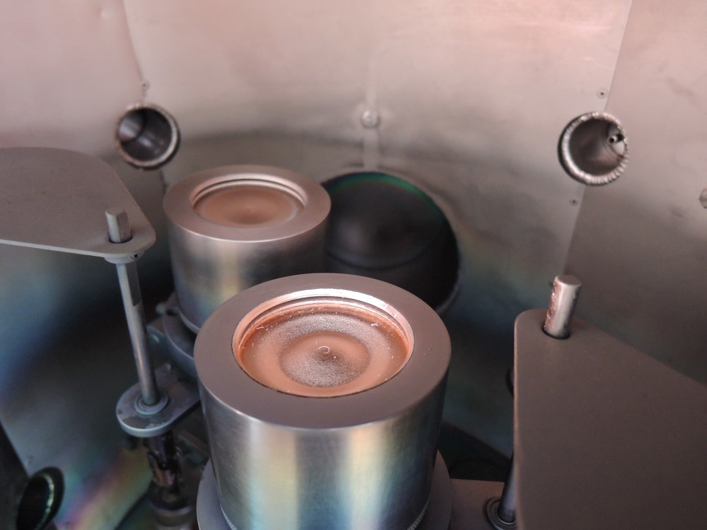
Image Credit: White_Fox/Shutterstock.com
What is Magnetron Sputtering?
Thin films play a crucial role in the fabrication of several components and devices, such as protective coatings, integrated circuits, solar cells, and optical/decorative/large-area coatings.
Precise control over the film composition, thickness, and uniformity and the ability to deposit different materials over several substrates are the other key advantages of this thin-film coating technology over other deposition techniques.
Sputtering involves the ejection of molecules/atoms from a solid target material due to the high-energy particle/ion bombardment. During this process, the kinetic energy from the incident ions is transferred to the targeted atoms, which results in a chain reaction of collisions within the target surface.
The targeted atoms are ejected from the target surface through evaporation when sufficient kinetic energy is transferred to overcome the binding energy of the targeted atom. Eventually, the ejected atoms can be deposited on an adjacent substrate.
In magnetron sputtering, positively charged ions, such as argon gas, are accelerated using an electric field towards a negatively charged target/cathode for targeted atom ejection. The ion bombardment process leads to both target atom removal and secondary electron emission from the sputtering target.
These emitted electrons can ionize the sputtering gas, which contributes to the plasma generation that sustains the entire sputtering process.
Factors Influencing the Sputtering Process
The sputtering process is primarily dependent on the mass of the ions, the angle of incidence, target atoms, and incident ion energy. Specifically, the sputtering yield relies on these factors and varies for different sputtering conditions and target materials.
Additionally, the number of target atoms ejected per incident ion is used to characterize the sputtering method efficiency. The ejected sputtered atoms from the target travel through low-pressure sputtering gas to reach the substrate, where these atoms condense and form a thin film.
The deposited thin film properties, such as composition and thickness, can be controlled by regulating the sputtering conditions, including the applied power/voltage, the sputtering gas pressure, and the distance between the substrate and the target.
Magnetic Sputtering Types and Key Parameters
Direct current (DC) magnetron sputtering, radio frequency (RF) magnetron sputtering, and high power impulse magnetron sputtering (HIPI) magnetron sputtering are the most common types of magnetron sputtering techniques used for thin film deposition.
A DC supply and an RF power supply are utilized to generate plasma within a low-pressure gas environment in DC magnetron sputtering and RF magnetron sputtering, respectively. The plasma is generated near the target material, which is primarily a ceramic/metal material.
Additionally, the magnetic assembly-generated magnetic field increases the sputtering rate and ensures higher uniformity in sputtered material deposition on the substrate. In HIPI magnetron sputtering, a series of high-power impulses generated using a pulsed power supply is applied to the target material.
The key magnetron sputtering parameters, including target power density, gas pressure, substrate temperature, and deposition rate, can critically influence the performance and quality of the deposited thin films. Optimized thin film deposition process, improved film quality, and thin films with desired properties can be realized by adjusting these parameters.
For instance, the desired sputtering rate and film quality can be achieved by optimizing the target power density. However, a higher target power density can increase the sputtering rate, leading to greater ionization and lower film quality.
Similarly, the gas pressure/substrate temperature and the deposition rate can be optimized to realize desired film quality and properties and film thickness and uniformity, respectively.
Thin Film Deposition Using Magnetron Sputtering
Pure metal-based thin films, alloy-based thin films, non-metallic compound-based films, and insulating thin films can be fabricated using different magnetron sputtering techniques.
For instance, molybdenum, tantalum, and niobium-based thin films with uniform distribution, low roughness, and high density can be deposited using an unbalanced DC magnetron sputtering technique.
Molybdenum thin films can significantly improve the scratch resistance of nickel-titanium shape memory alloys. Similarly, RF magnetron sputtering is used extensively in the direct fabrication of insulting thin films, such as niobium (V) oxide/molybdenum trioxide films.
In a study published in Applied Physics Letters, researchers employed the RF magnetron sputtering technique to fabricate thin-film transistors (TFTs) using amorphous indium gallium zinc oxide (a-IGZO) channels at room temperature. The a-IGZO film conductivity was controlled from 10−3 to10−6 S cm−1 by varying the mixing ratio of the sputtering gases oxygen/oxygen+argon from 3.1% to 3.7%.
Researchers successfully operated the top-gate-type TFTs in n-type enhancement mode with 12 cm2 V-1 s-1 field-effect mobility, an on-off current ratio of 108, and 0.2 V decade-1 subthreshold gate voltage swing, which demonstrated the feasibility of using a-IGZO as a semiconductor material to fabricate high-mobility TFTs at low temperatures on flexible substrates.
In another study published in the journal Applied Physics Letters, researchers fabricated zinc oxide TFTs on silicon substrates using RF magnetron sputtering at near room temperature.
The best devices demonstrated a field-effect mobility of over two cm2/V s and an on-off ratio of more than 106. These zinc oxide films also displayed 105 ohm cm with high optical transparency of over 80% for wavelengths higher than 400 nm and less than 0.5 GPa compressive stress.
Thus, low-temperature processing, exceptional transistor characteristics, and high transparency in the visible range make the synthesized zinc oxide TFTs suitable for flexible electronics on temperature-sensitive substrates.
More from AZoM: What are the Best Anti-Corrosion Thin Films?
References and Further Reading
Carcia, P. F., McLean, R. S., Reilly, M. H., Nunes, G. (2003). Transparent ZnO thin-film transistor fabricated by rf magnetron sputtering. Applied Physics Letters, 82(7), 1117–1119. https://doi.org/10.1063/1.1553997
Yabuta, H., Sano, M., Abe, K., Aiba, T., Den, T., Kumomi, H., Nomura, K., Kamiya, T., Hosono, H. (2006). High-mobility thin-film transistor with amorphous InGaZnO4 channel fabricated by room temperature rf-magnetron sputtering. Applied Physics Letters, 89(11), 112123. https://doi.org/10.1063/1.2353811
Li, J., Ren, G. –K., Chen, J., Chen, X., Wu, W., Liu, Y., Chen, X., Song, J., Lin, Y. –H., Shi, Y. (2022) Facilitating Complex Thin Film Deposition by Using Magnetron Sputtering: A Review. JOM, 74, 3069–3081. https://doi.org/10.1007/s11837-022-05294-0
Abbas, N. (2023). Magnetron Sputtering: A Versatile Thin Flim Deposition Technique [Online] Available at https://www.wevolver.com/article/magnetron-sputtering-a-versatile-thin-flim-deposition-technique (Accessed on 10 August 2023)
Disclaimer: The views expressed here are those of the author expressed in their private capacity and do not necessarily represent the views of AZoM.com Limited T/A AZoNetwork the owner and operator of this website. This disclaimer forms part of the Terms and conditions of use of this website.