Thin-film electronic devices constructed with flexible materials like plastics, polymers, and metals are gaining increased popularity. Their ability to bend, fold, and roll, coupled with their lightweight structure and durable nature, makes them perfect for many applications. These applications include smart bandages, wearable devices, and foldable displays.
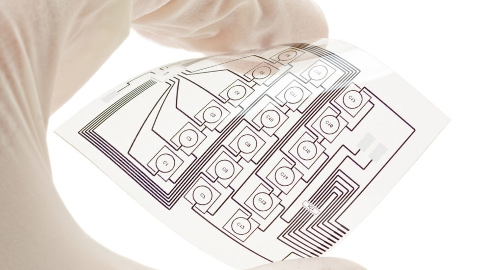
Image Credit: Harrick Plasma
These devices can be manufactured using many methods, such as printing, coating, and lamination. Flexible electronics offer several potential benefits over conventional electronic devices due to their high performance, flexibility, low cost, and process simplicity.
Plasma treatment plays a crucial role in the manufacturing of thin-film electronics. The advantages of plasma treatment for thin-film electronics include:
- Enhancing surface roughness can improve adhesion between materials. This becomes especially important in flexible electronics, ensuring proper adherence between different layers of the device.
- Generating reactive functional groups can improve chemical bonding between materials. This can be utilized to create a surface that is more compatible with other materials, such as solvents or adhesives.
- Eliminating contaminants from a surface enhances the quality of the final product. This is important in flexible electronics, as it prevents defects and ensures the device's proper functioning.
Bioelectronics
Bioelectronics form a subset of thin-film electronics, combining flexible wearable electronics with biomedical applications. A commonly used material for these devices is poly(3,4-ethylenedioxythiophene) polystyrene sulfonate (PEDOT:PSS).
This material boasts several beneficial properties, including high conductivity, low cost, chemical stability, and non-toxicity. It is suitable for flexible electronics because it can easily mold into different shapes.
In the fabrication of these devices, plasma exposure is used to modify material surfaces before the deposition of PEDOT:PSS. This plasma treatment modifies the surface by eliminating contaminants and enhancing its hydrophilicity.
This alteration makes the surface more conducive to the spin-coating process, allowing the deposition of the desired layer for flexible electronics.
For example, in a study by Chen et al. (2022), a polydimethylsiloxane (PDMS) substrate underwent plasma exposure to impart hydrophilicity to the surface, ensuring proper adhesion. Following the plasma treatment, silver nanowires (AgNWs) and PEDOT:PSS were deposited on the surface.
The resultant device was a “self-cleaning flexible wearable temperature sensing device,” enabling real-time temperature monitoring of patients. The tracking of various health information parameters is a common aspect of bioelectronics since it helps in making healthcare more patient-friendly.
Other Devices
As the popularity of thin-film electronics continues to grow, there is a corresponding increase in the variety of materials used for their fabrication. These materials include graphene, PDMS, and carbon nanotubes (CNTs).
Recent articles have highlighted the use of Harrick Plasma devices to create a variety of thin-film electronics:
- Thin-film wearable heaters were fabricated to enhance the existing rigid and heavy heaters used in therapeutic care. Silica and indium-tin-oxide (ITO) substrates underwent plasma treatment before being coated with PDMS. The pre-treatment with plasma promoted the covalent binding of the thin films to the cured PDMS layer (Ding and Moran-Mirabel 2022).
- A graphene-based wearable electronic device was developed to track subtle skeletal muscle movements for disease diagnostics. The device featured an ultra-soft, super-compressible graphene-based cellular material (UGCM). However, during mechanical testing, failures easily occurred in the UGCM. To address this issue, two PDMS pieces were plasma treated and bonded to the UGCM, forming a sandwich structure. This alteration prevented material failures, allowing the device to be suitable for wear (He et al. 2022).
References and Further Reading
Featured Bioelectronics Articles
- Chen CH, Tsai TW, Cheng IC, Chen JZ. “Superhydrophobic, Oleophobic, Self-Cleaning Flexible Wearable Temperature Sensing Device”. ECS Advances (2022) 1: 036502. 10.1149/2754-2734/ac82bf 10.1149/2754-2734/ac82bf
- Chen H, Yang W, Zhang C, Wu M, Li W, Zhou Y, Lv L, Yu H, Ke H, Liu R, Xu Y, Wang J, Li Z. “Performance-enhanced and cost-effective triboelectric nanogenerator based on stretchable electrode for wearable SpO2 monitoring”. Nano Research (2022) 15: 2465-2471. 10.1007/s12274-021-3724-1
Other Devices Articles
- Abunala H, Zafar H, Anjum D, Alazzam A, Mohammad B. “Enhanced Graphene Oxide Electrical Properties for Thin-Film Electronics Using an Active/Shrinkable Substrate”. ACS Omega (2023) 8: 1671-1676. 10.1021/acsomega.2c07306
- Ding X, Moran-Mirabal J. “Efficient Multi-Material Structured Thin Film Transfer to Elastomers for Stretchable Electronic Devices”. Micromachines (2022) 13. 10.3390/mi13020334
- He Z, Qi Z, Liu H, Wang K, Roberts L, Liu J, Wang S, Cook M, Simon G, Qiu L, Li D. “Detecting subtle yet fast skeletal muscle contractions with ultrasoft and durable graphene-based cellular materials”. National Science Review (2022) 9: nwab184. 10.1093/nsr/nwab184
- Khakbaz H, Ruberu K, Kang L, Talebian S, Savyar S, Filippi B, Khatamifar M, Beirne S, Innis P. “3D printing of highly flexible, cytocompatible nanocomposites for thermal management”. Journal of Materials Science (2021) 56. 10.1007/s10853-020-05661-9
Supplemental Articles (Not Featuring Harrick Plasma Cleaners)
- Sahoo BN, Janghoon W, Algadi H, Lee J, Lee T. “Superhydrophobic, Transparent, and Stretchable 3D Hierarchical Wrinkled Film-Based Sensors for Wearable Applications”. Advanced Materials Technologies (2019) 4: 1900230. 10.1002/admt.201900230

This information has been sourced, reviewed, and adapted from materials provided by Harrick Plasma.
For more information on this source, please visit Harrick Plasma.