When preparing cross sections, the standard procedure using the FIB-SEM technique is the use of high currents to quickly remove material, then lower the FIB current for an improved beam profile and final surface quality. However, decreasing the maximum current used for the final polishing of the section surface results in a longer preparation procedure.
For smaller cross-sections (tens of μm in size), this reduction technique is suitable. However, as the size of the cross-sectional area to be polished gets larger, there is a substantial increase in analysis time. This method is thus unsuitable for preparing cross-sections with sizes in the hundreds of μm. To overcome the limitation for bigger cross sections, plasma FIB was created to provide higher beam currents than those attainable with traditional Ga FIB-SEMs.
TESCAN Workflow For Getting Maximum Throughput and Artifact-Free Surfaces
Ga FIB-SEM and Xe plasma FIB-SEM both support multiscale investigations. The Ga FIB-SEM’s maximum current is around 100 nA, so it is best suited to material removal or the preparation of cross-sections in the range of tens of micrometers.
If a larger cross-section is needed, the Xe plasma FIB is a good solution, as it can reach up to 3 μA maximum FIB current and prepare bigger areas in the range of hundreds of micrometers. The higher throughput for sample characterization is achieved by combining high current sample polishing with methods of improving final sample cut quality.

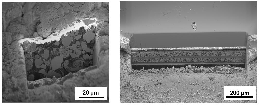
Cross section 500 µm wide and more than 300 µm deep prepared to visualize layers of MLCC electronic component. Image Credit: Tescan USA Inc.
TESCAN has developed innovative techniques that expedite sample processing by enhancing sample quality attained by higher polishing currents. The unique methods of TESCAN TRUE-X- Sectioning and TESCAN Rocking effectively mitigate artifacts from polishing.
The ideal workflow for high throughput sample characterization would combine high current FIB-SEM polishing, the TESCAN TRUE-X- Sectioning method, and the TESCAN Rocking Stage.
Large Area Characterization
Comparison of typical cross section sizes for Ga FIB SEMs Left and plasma Xe FIB SEMs Right Right image 50 µm wide cross section of a Li ion battery electrode prepare by Ga FIB SEM Left image 1 mm wide cross section of a Li ion battery electrode prepare by plasma FIB SEM. Image Credit: Tescan USA Inc.
Preparation of Artifact-Free Cross Section Surface

Images comparing cross section surface quality before and after application of specific technique for artifact removal. Right image – Application of TESCAN TRUEX-Sectioning for ripples reduction. Left image – Application of TESCAN Rocking stage for curtaining removal from polished surface. Image Credit: Tescan USA Inc.
Artifacts on the polished surface area of a sample occur because of the interaction of ions with the sample. They are material dependent. Over time, two typical artifacts have become apparent registering two typical artifacts—Ripples (terraces) and Curtaining. Traditionally, the method used to mitigate these artifacts is to reduce the polishing FIB current that impacts the final preparation time.
Techniques masking (TESCAN TRUE-X-Sectioning] and rocking polishing (TESCAN Rocking Stage) can be employed to reduce the curtaining and ripples from polished surfaces while maintaining a high material sputter rate.
Application of TESCAN TRUE X Sectioning Method
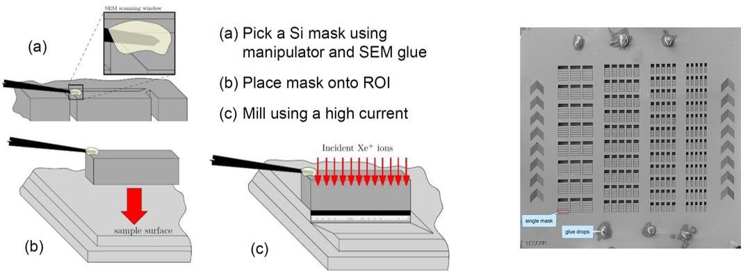
Left image: Schematic drawing of manipulation and use of the TESCAN TRUE X Sectioning method using Si masks instead of protective layer 1. Right image: SEM image of prefabricated Si masks for use in FIB SEM Application of TESCAN Rocking stage method. Image Credit: Tescan USA Inc.
Application of TESCAN Rocking Stage Method
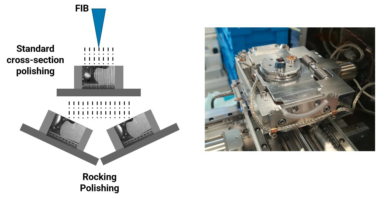
Left image: Schematic drawing of rocking polishing method performed by TESCAN Rocking stage. Right image: TESCAN Rocking Stage. Image Credit: Tescan USA Inc.
Effect of Higher Currents on Final Preparation Time

Image Credit: Tescan USA Inc.
Above is a graphical representation of cross-section preparation time derived for theoretical cross-sections of 10x10 μm and 50x10 μm in size. The second example demonstrates that preparation time will increase when the larger cross-section (50x10 μm) is prepared, even under the same conditions applied to a smaller cross-section of 10x10 μm.
The same currents were utilized for the larger cross-section due to the optimization of the FIB beam currents for the specific material. To achieve the same polished surface quality, the same FIB beam currents must be applied to the large cross-section.
The last example demonstrates the reduction in time when a marginally higher FIB current is used for polishing, particularly in the final step of polishing, which is the most time-consuming aspect of cross-section preparation.
Conclusions
It is important in materials characterization to use larger areas to deliver an improved statistical representation and discover greater contextual information about the material. It is essential to minimize sample preparation time for effective characterization of large areas. FIB-SEM can characterize specimens at specific sample sites due to its highly precise navigation to the area of interest and exacting milling.
When it comes to the throughput of the sample preparation in FIB-SEM, the final polishing step is crucial. The polishing conditions greatly depend on the properties of the material and the current used for the final polishing must be optimized for high-quality sample preparation with the highest current possible. This experiment proves that the highest current can be used in combination with TESCAN TRUE-X-Sectioning and TESCAN Rocking Stage, achieving excellent results in a short amount of time.

Image Credit: Tescan USA Inc.
References and Further Reading
- Tomáš Hrnčíř, Marek Šikula, Jozef Oboňa & Pascal Gounet: “How to achieve artefact-free FIB milling on polyimide packages”, ISTFA 2016 Conference proceedings, pg. 642-646

This information has been sourced, reviewed and adapted from materials provided by TESCAN USA Inc.
For more information on this source, please visit TESCAN USA Inc.