OkyayTech Layerava® features a compact reactor design with a large plasma source.
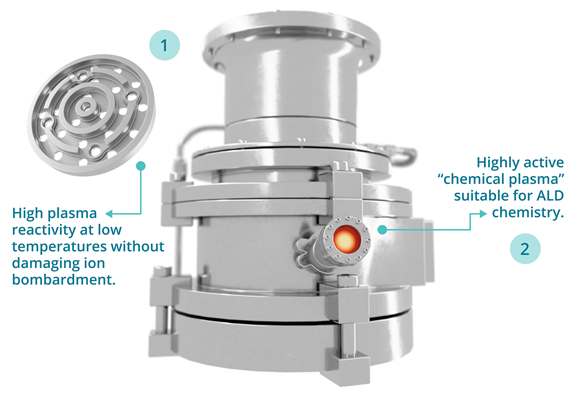
Image Credit: OkyayTech ALD
Choose Layerava® HCPE-ALD
Layerava® Hollow Cathode Plasma Enhanced Atomic Layer Deposition
- No oxygen contamination
- No plasma damage
- Faster growth rate
- Better crystal quality
- Reduce complexity
Process Performance and Film Quality
- Pure films
- Device reliability
- Lower deposition time
- Electrical improvement
System Design and Complexity
Get in touch now
Market and Technology
Common plasma sources, such as CCP and ICP, were created decades ago for use in the semiconductor industry. At that time, plasma sources were primarily used to deposit silicon oxide and silicon nitride. Today, novel materials face increasingly stringent demands in the expanding industry, particularly for plasma-assisted atomic layer deposition (ALD).
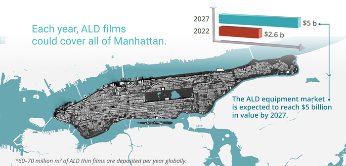
Image Credit: OkyayTech ALD
Traditional plasma-assisted ALD approaches have drawbacks such as oxygen contamination, plasma damage, and complicated system requirements. Hollow cathode plasma-assisted ALD is the most promising prospect for addressing those issues in a single system.
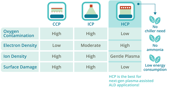
Image Credit: OkyayTech ALD