In this interview, the Director of Sales at Photon etc., Laura-Isabelle Dion-Bertrand, speaks with AZoM about how spectral imaging can help enhance the next generation of solar cells.
What is hyperspectral imaging, and what can be measured using this technique?
Hyperspectral imaging is a non-invasive spectroscopy technique that produces extensive three-dimensional datasets (or data cube), where each pixel contains a unique spectrum. In this method, the X-Y axis indicates spatial information, while the Z-axis represents spectral data.
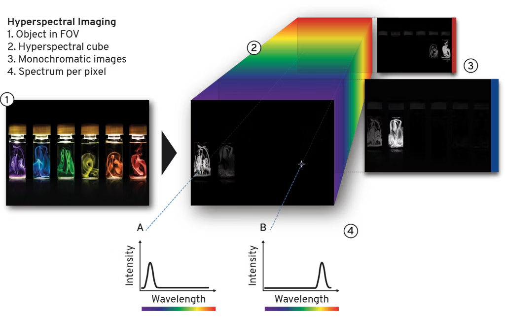
Image Credit: Photon etc.
This versatile technique enables a broad spectrum of optical measurements, including but not limited to electroluminescence (EL), steady-state and time-resolved photoluminescence (PL), Raman spectroscopy, standard transmittance, reflectance, and darkfield microscopy.
Could you please provide some information about Photon etc.’s hyperspectral technology and highlight what distinguishes it from other technologies available in the market?
Numerous hyperspectral systems currently in use in the market utilize single-point (raster scan) or line-scan (push-broom) imaging methodologies. In these methods, either the samples or the hyperspectral instrument must move with respect to each other to produce hyperspectral data cubes.
At Photon etc., we offer two distinct hyperspectral platforms:
- The L-EOS: A push-broom hyperspectral camera specifically designed for in-line inspection purposes. Objects under inspection are usually moving on a linear translation stage or a converyor belt.
- The IMA or GRAND-EOS: Global or wavelength scanning hyperspectral imaging systems utilize patented Volume Bragg Grating (VBG) filtering technology to sequentially capture monochromatic images. These platforms were specifically crafted with an emphasis on fundamental research and acquiring insights into the optical properties of advanced materials. They are ideal for the fast acquisition of spectral information from millions of points in the field of view of the camera.
While both imaging techniques have their own strengths and weaknesses, for this interview, our focus will be directed toward the technology underpinning IMA and GRAND-EOS, specifically the global hyperspectral imaging approach.
As mentioned, the filtering technology that underpins IMA and the GRAND-EOS is reliant upon volume Bragg gratings (VBG). A VBG is a diffraction grating characterized by a periodic modulation of the refractive index spanning its entire volume.
In the platforms that we have created, VBGs are positioned on a rotation stage within the Hypercube (as depicted in the accompanying figure) to enable the selection of various wavelengths.
The Hypercube, Photon etc's tunable imaging filter, can be seamlessly integrated into a conventional scientific-grade microscope or coupled with standard collection optics. Positioned in front of the sensor, it can accommodate a sCMOS camera, an InGaAs camera, or both simultaneously, effectively expanding the spectral range coverage.
VBGs filter the entire field of view (FOV) for each camera snapshot, thereby enabling global imaging. This technique requires uniform illumination (e.g., by LEDs, lasers, white light, etc.) throughout the entire FOV while concurrently capturing the emitted signal from each point within the FOV. As a result, this approach effectively eradicates any artifacts arising from image reconstruction.
For PV research applications, homogeneous illumination can be used to create an iso-potential for photogenerated carriers, effectively minimizing their diffusion towards darker, unilluminated regions. This is critical when studying PV materials in complete devices as some operational parameters like charge-depletion width and photoinduced bias are non-locally dependent on the illumination conditions. Global imaging also enables photoluminescence (PL) experiments to be conducted within a realistic operating range of 0.1 suns to 500 suns, which PV materials will experience in the field.
A unique aspect that differentiates our platforms apart is the quantitative nature of the measurements they offer. This means that we can provide photoluminescence (PL) and electroluminescence (EL) data in calibrated units of photon/eV·s·cm2·sr (see example below) rather than relying on arbitrary units. This feature provides quantive maps of parameters of critical parameters such as the External Quantum Efficiency (EQE) and the Quasi-Fermi Level Splitting (QFLS).
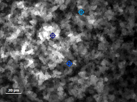
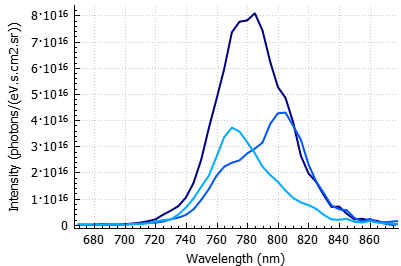
Left: Monochromatic PL image @785 nm of perovskite crystals aged in air excited at 532 nm. Right: Quantitative PL spectra extracted from hyperspectral data.
Image Credit: Photon etc.
What value does hyperspectral imaging bring to the table during the development of new photovoltaic materials?
Global hyperspectral imaging provides invaluable insights into the exploration of emerging photovoltaic materials by offering comprehensive spectral and spatial data under realistic conditions of illumination.
Photoluminescence (PL) and electroluminescence (EL) are well-established and widely recognized non-destructive techniques that provide insights into a given sample’s optical and electronic properties, material quality, and device performances. PL and EL can also offer key information on material uniformity and composition, carrier generation efficiency and their recombination pathways, band-gap variations, and electronic defects characterization.
Absorbance and reflectance measurements yield valuable insights into the optical characteristics and performance of solar materials. These techniques provide essential information, including band-gap determination, optical losses, material uniformity, and light energy conversion efficiency.
Darkfield spectroscopy, also available on our IMA platform, is a measurement technique that can provide valuable information on the scattering and surface properties of photovoltaic materials. It allows for the investigation of parameters such as surface morphology, scattering mechanisms, light-trapping effects, and the presence of surface contaminants.
Integrating hyperspectral imaging with these techniques introduces spatial dimensions to the data they offer, enabling the evaluation of:
- The spatial distribution of electronic defects, impurities, and variations in material composition.
- The influence of a material’s micro and macrostructure on carrier generation, recombination, and transport.
- The efficacy of light trapping and surface passivation strategies implemented in the device.
All of the above aid in the optimization of material quality, efficiency, and performances.
It is crucial to highlight that many luminescence imaging characterization techniques provide data in arbitrary units, which can limit their interpretability due to the absence of quantitatvie information. With this in mind, researchers at IRDEP (now IPVF, France) have designed a patented method for spectral and photometric calibration.1
This technique has been implemented in Photon etc.’s platform and allows data on the absolute number of photons emitted at a specific energy from every point on the sample’s surface to be obtained.
Through this calibration process, researchers can leverage Planck’s law and the reciprocal relationships among a solar cell’s External Quantum Efficiency (EQE), its Electrolumine5scence (EL) emitted at a specific voltage, or its Photoluminescence (PL) under a defined illumination density.2
Hyperspectral photometric calibrated data contributes to meaningful scientific findings, enabling in-depth interpretation by providing maps of parameters such as:
- Charge transport efficiency3
- External Quantum Efficiency (EQE)
- Quasi-Fermi Level Splitting (Δμ)1,3
- Saturation current4
- The local voltage of the diode
In addition to these unique benefits, hyperspectral imaging already plays a substantial role in guiding the advancement and enhancement of photovoltaic materials by delivering crucial insights into their optical properties and performance.
For instance, in the work by Hamadani et al.5, it was found that hyperspectral luminescence imaging on dilute-alloy InGaAs solar cells can be used to identify and investigate dark spots and the locally high concentration of radiative defects at their center, as well as systemic variations of the luminescence pattern across the device.
In a Nature publication by Y. Sun et al.6, researchers from University of Cambridge and University of Science and Technology of China (Hefei) joined forces to demonstrate perovskite light-emitting diodes in the near-infrared spectral range.
How does your technology adapt to the wide array of emerging photovoltaic materials in existence?
Photon etc.’s hyperspectral imagers are designed with modularity in mind, providing researchers with a versatile tool for their experiments. The intrinsic configuration offers fundamental specifications that facilitate PL measurements using high-power LEDs and transmittance measurements in either the visible range (400-1000 nm) or the infrared range (900-1650 nm).
To accommodate the unique research needs of various groups, departments, or research centers, several add-ons are available (see the figure below).
The instrument’s spectral range extension from 400 to 1650 nm allows for the characterization of a wide range of candidate materials for next-generation solar cells such as perovskites, GaAs, CIS, CIGS. The use of sensitive sCMOS and InGaAs cameras permits even the faintest of signals to be observed.
The system also facilitates the integration of multiple excitation wavelengths within a single platform, enabling the examination of various band-gap materials and tandem cells. For applications that require higher power density, high-power lasers can be added instead of LEDs. LEDs are restricted to delivering the equivalent of one sun’s worth of power to the sample, whereas laser-based illumination can achieve intensity levels ranging from dozens to hundreds of suns.
A motorized stage can also be included to enhance functionality, facilitating automated measurements and stitching capabilities to accommodate different sizes of samples or devices. Using Photon etc.’s proprietary software, users can program complex experimental sequences that the system will execute automatically without requiring any intervention from lab personnel.
Additional options include:
- Absolute calibration module (which provides the advantages described in question 3)
- Polarization measurements
- Epifluorescence module
- The electroluminescence station, including probes and source meter, is all integrated within the acquisition software
- Darkfield module
These options enable researchers to customize this hyperspectral characterization platform to align with their unique requirements, thus simplifying a broad spectrum of scientific inquiries in an efficient fashion.
How can the effective integration of hyperspectral imaging be incorporated into various stages of the solar cell development process?
During the initial stages of material development, hyperspectral microscopy can help users better understand fundamental properties at a microscopic scale.
Our hyperspectral imaging platform, by offering maps of defect distribution, composition uniformity, photoluminescence quantum yield, and various optoelectronic properties, empowers users to choose the most suitable fabrication method to improve the efficiency of their photovoltaic materials, and our IMA system delivers this comprehensive analysis, empowering researchers with valuable insights.
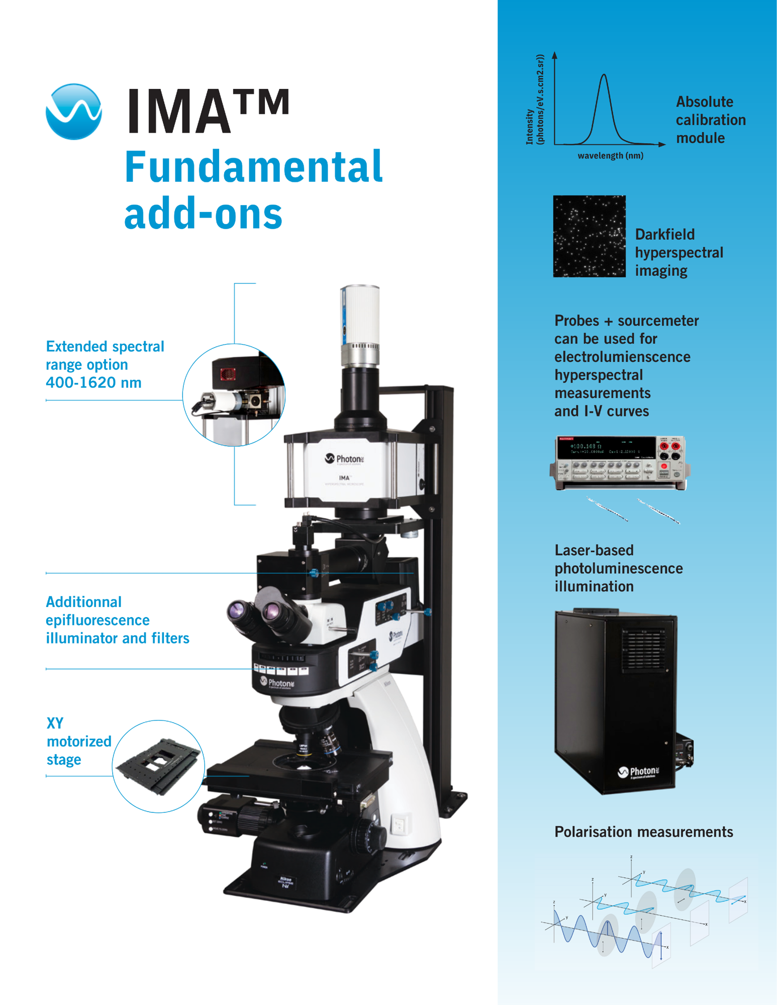
Image Credit: Photon etc.
As solar materials progress from small-scale devices to standardized modules, the fabrication processes must be scaled up, all while ensuring reproducibility and reliability. In this context, conducting spectral analysis on a broader scale becomes essential for evaluating process uniformity and the overall performance of the module.
EL and PL hyperspectral mapping is a powerful tool for evaluating module degradation during environmental stress testing or routine field operations.
Our GRAND-EOS system is specifically engineered for this purpose, facilitating spectral analysis at a larger scale (2x2 cm2, 22x22 cm2) to validate material consistency, enhance manufacturing processes, evaluate production quality, and monitor module deterioration.
By effectively integrating hyperspectral imaging at every stage of solar cell development, scientists and engineers can directly observe the impact of their design strategies at both the microscale and the module level. This approach offers immediate feedback on the efficacy of these strategies, expediting the progress of solar cell technologies. Ultimately, this contributes to the development of efficient, reliable, and commercially viable solar energy solutions.
What is next in terms of development for your platform?
Our roadmap results from collaboration between Photon etc., and our customers, who consist of researchers working on the advancement of next-generation solar materials and companies involved in the commercialization of photovoltaic solutions.
Our team is currently investigating a time-resolved photoluminescence (TRPL) hyperspectral imaging platform. TRPL analysis of solar materials offers crucial information about carrier dynamics, defect characteristics, material quality, charge carrier transport, and interface properties.
The synergistic approach of combining TRPL and imaging capabilities will allow for a comprehensive understanding of the material’s optical and electrical properties, facilitating the identification of performance-limiting factors, the optimization of device designs, and the development of more efficient solar cells.

Image Credit: Photon etc.
We have also recently added a cryogenic option to our hyperspectral microscopy platform. Cryogenic spectroscopic measurements of solar materials offer a temperature-dependent analysis, suppressing thermally activated processes and reducing spectral broadening.
Lastly, we are presently in the process of developing a quality control tool to address a crucial aspect of solar panel manufacturing. As solar panels reach the market, it becomes crucial to incorporate non-destructive, in-line quality control techniques to ensure the final products meet the desired specifications.
Our L-EOS, initially designed for core drill in-line inspection, can be readily adapted for use in the field of photovoltaics, offering an efficient and dependable solution for quality control. With the L-EOS, real-time monitoring and inspection can be carried out to guarantee the panels’ overall performance and compliance.
Where can our readers go to find out more?
Readers can access more information in the dedicated section on our website focused on solar materials.
Our products dedicated to material sciences are also available here.
Finally, the list of peer-reviewed scientific papers in the field of photovoltaics can be found here.
About Laura-Isabelle Dion-Bertrand
Laura-Isabelle serves as the Director of Sales at Photon, overseeing and guiding the sales team toward achieving their objectives. In addition to her sales leadership, she plays a pivotal role in strategic development and marketing initiatives to drive the company's growth and success.
Laura-Isabelle holds a Bachelor of Science degree in Physics from the Université de Montréal. She further pursued her academic journey at the same institution, obtaining a master's degree in Condensed Matter Physics with a research focus on charge separation in organic photovoltaics.
Her profound expertise in material science has resulted in numerous publications in collaboration with esteemed researchers worldwide. Laura-Isabelle's in-depth knowledge has unlocked
About Photon etc.
Photon etc. is a renowned Canadian-Quebec company, located in the heart of Montreal's innovative district, specializing in the design and manufacturing of hyperspectral and infrared imaging systems. Founded in 2003, our expertise in photonics allows us to provide innovative solutions to the most complex challenges of research and advanced industrial applications.
Scientists and industry alike turn to our expertise for the most advanced imaging and analysis instruments, whether it's to discover new materials for solar energy, see-through living tissue, or obtain the best characterization of an industrial product. This is reflected in the growing number of scientific publications that use our products for their research.
We focus our efforts on three specific sectors: industrial, advanced materials, and life sciences.
We want to hear more about your research. Contact us to start a discussion: [email protected].
References
1. Delamarre A. , Paire M., Guillemoles J.-F. and Lombez L., Quantitative luminescence mapping of Cu(In,Ga)Se2 thin-film solar cells, Progress in Photovoltaics, 2014.
2. Rau, U., Reciprocity relation between photovoltaic quantum efficiency and electroluminescent emission of solar cells, Physical Review B 76(8), 2007.
3. El-Hajje, G., Momblona, C., Gil-Escrig, L., Ávila, J., Guillemot, T., Guillemoles, J.-F., Sessolo, M., Bolink, H. J., & Lombez, L. (2016). Quantification of spatial inhomogeneity in perovskite solar cells by hyperspectral luminescence imaging. In Energy & Environmental Science (Vol. 9, Issue 7, pp. 2286–2294). Royal Society of Chemistry (RSC). https://doi.org/10.1039/c6ee00462h
4. Delamarre, A., Lombez, L., & Guillemoles, J.-F. (2012). Contactless mapping of saturation currents of solar cells by photoluminescence. In Applied Physics Letters (Vol. 100, Issue 13). AIP Publishing. https://doi.org/10.1063/1.3697704
5. Conrad, B., & Hamadani, B. H. (2023). Identifying and investigating spatial features in InGaAs solar cells by hyperspectral luminescence imaging. In AIP Advances (Vol. 13, Issue 3, p. 035318). AIP Publishing. https://doi.org/10.1063/5.0131691
6. Sun, Y., Ge, L., Dai, L., Cho, C., Ferrer Orri, J., Ji, K., Zelewski, S. J., Liu, Y., Mirabelli, A. J., Zhang, Y., Huang, J.-Y., Wang, Y., Gong, K., Lai, M. C., Zhang, L., Yang, D., Lin, J., Tennyson, E. M., Ducati, C., … Greenham, N. C. (2023, March 15). Bright and stable perovskite light-emitting diodes in the near-infrared range. Nature News. https://www.nature.com/articles/s41586-023-05792-4

This information has been sourced, reviewed and adapted from materials provided by Photon etc.
For more information on this source, please visit Photon etc.
Disclaimer: The views expressed here are those of the interviewee and do not necessarily represent the views of AZoM.com Limited (T/A) AZoNetwork, the owner and operator of this website. This disclaimer forms part of the Terms and Conditions of use of this website.