Sponsored by TescanReviewed by Ify IsiborNov 17 2026
A typical physical failure analysis workflow consists of delayering through chip deprocessing, defect localization using electrical characterization techniques such as nanoprobing and conductive AFM, and defect characterization through TEM-based imaging and materials analysis.
The deprocessing and electrical characterization stages have traditionally required the use of several instruments.
Conventional deprocessing methods are relatively coarse, provide limited localized control, and often leave a rough surface finish. In contrast, site-specific deprocessing and electrical characterization can now be performed on a single platform using the TESCAN AMBER X plasma FIB-SEM.
Achieving excellent surface planarity (below 5 nm RMS roughness) is critical for straightforward nanoprobe access while minimizing foreign ion implantation that could alter the device’s electrical behavior.
The high-resolution imaging capabilities of the BrightBeam™ SEM column improve ultra-low-keV imaging performance and facilitate identification of defective interconnects through passive voltage contrast (PVC).
High-resolution live imaging at 200 eV and 500 eV with beam currents below 40 pA, combined with Kleindiek’s Probe Shuttle PS8 in situ nanoprobing system, enables direct I-V characterization.
This capability provides valuable insight into defect behavior and device functionality in structures such as PMOS and NMOS transistors within sub-20 nm technologies.
The TESCAN AMBER X combines a dual-beam architecture with the BrightBeam™ SEM column, delivering exceptional ultra-low-keV imaging performance at beam energies of 500 eV and 200 eV and beam currents as low as 40 pA, without requiring beam deceleration.
The system also incorporates the latest iFIB+™ Xe+ plasma FIB, offering beam energies from 30 keV down to 3 keV and currents ranging from 1 pA to 2 µA, supporting a broad spectrum of applications.
The Xe+ plasma FIB-SEM platform is particularly well-suited for several critical semiconductor failure analysis tasks, with delayering being one of its most important applications.
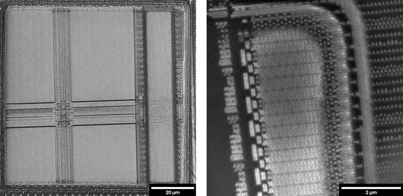
Gas-assisted delayering of a 10 nm node process with Xe plasma FIB. (Left) Overview of a 100 × 100 μm2 delayered window. (Right) Layer of interest imaged at 200 eV. Image Credit: Tescan
The introduction of Xe+ plasma-focused ion beam technology, together with TESCAN’s specialized A-Maze and Nanoflat chemistries, has transformed the delayering process. It is now possible to achieve highly localized, smudge-free, and extremely planar results while opening comparatively large regions (100 × 100 µm2 or larger) on advanced semiconductor devices.
An important advantage of xenon (Xe) is its inert nature, which prevents the formation of intermetallic compounds during milling. As a result, key electrical characteristics such as conductivity remain unchanged, ensuring that subsequent electrical measurements are not influenced by parasitic FIB-induced electrical effects.
Accurate end-point detection (EPD), based on the secondary electron signal generated by the FIB, provides precise control throughout the delayering process and allows milling to stop at the desired layer for inspection or electrical probing.
Contamination associated with low-kV SEM imaging can also be effectively managed through the use of low electron beam currents and a decontamination system.
Together, these capabilities establish the TESCAN AMBER X as a preferred platform for deprocessing sub-20 nm technology nodes, supporting FEoL development workflows in modern semiconductor fabrication facilities and foundries.
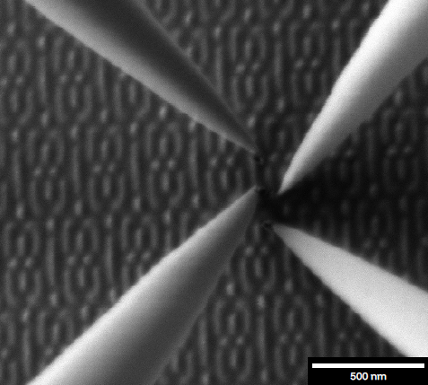
PMOS measurement on SRAM transistor bits on 10 nm technology acquired at 500 eV. Image Credit: Tescan
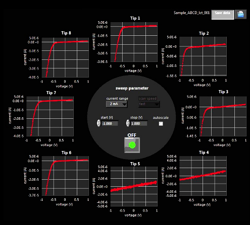
Six probes acquiring transistor functionality on the Kleindiek’s PS8 control panel. Image Credit: Tescan
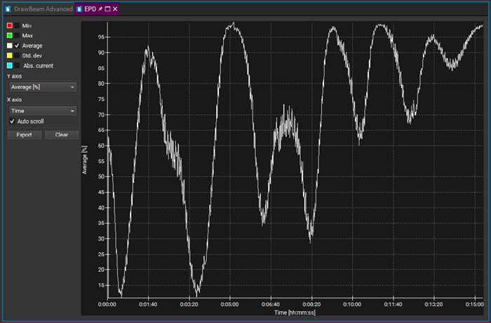
Precise EPD is implemented by collecting and plotting the SE signal, which assists in monitoring and controlling the delayering process. Each peak corresponds to a metal layer, while minima correspond to via layers. Image Credit: Tescan

This information has been sourced, reviewed, and adapted from materials provided by Tescan.
For more information on this source, please visit Tescan.