Introduction A new type of the flat displays, such as electroluminescence displays and field emission displays (FEDs), attracts many interests. Among them, FEDs have many similarities with conventional cathode ray tubes (CRTs). As for the FEDs and CRTs, electrons are accelerated in vacuum towards phosphors that then glow. The main difference is that the electrons are generated from the cold emitter rather than the thermal emitter so the device consumes much less power and can be turned on instantly. Instead of one single electron gun, each pixel comprises several thousands sub-micrometer tips from which electrons are emitted. To achieve a low operating voltage of the cold emitter, the tip is manufactured into very sharp form so that the local field strengths become high enough for even a moderately low gate voltage. It is also made of a low-work function material such as molybdenum. To confirm the advantage of sharp tip working, Spindt et al. [1] measured that emission originated from the tip of molybdenum cones with an about 1.5 μm in tall and 50 nm in a tip radius was the maximum current of 50~150 μA per cone at the applied voltages in the range of 100~300 V. In addition, Saito et al. [2] investigated behavior of field emission from open multi wall carbon nanotubes (MWNTs). The current density in the rage of 10~100 μA/cm2 was obtained. It is well known that diamond and amorphous carbon and related films are low-work function materials. For example, hydrogenated diamond (111) surface has the negative electron affinity of –1.3 eV [3, 4]. Mueller et al. [5] prepared the diamond array, and evaluated behavior of field emission. The emission current of 3.5 mA was achieved at 0.8 V/μm in this configuration. Satyanarayana et al. [6] showed that the threshold fields of 3~5 V/μm was obtained at the current density of 1 μA/cm2 from the amorphous carbon (a-C) films. Furthermore, Huq et al. [7] prepared an array of Si tips with the a-C film coating. They reported that a maximum current of 50 μA was obtained with an applied field strength of 2.25 V/μm. The carbon and related materials with the sharp tips are the most important candidate for the field emission element. Our research group develops the aggregation of the ceramic whiskers on the silicon and other solid-state materials [8-14]. The ceramic field emitter was formed by the electrically conductive whisker with the sharp tip and amorphous carbon and related coating with relatively low-work function. For example, a performance of the diode display operated by the cold emitter formed from aluminum-doped ZnO (Al:ZnO) whiskers coated with amorphous hydrogenated carbon nitride (a-CNx:H) films was reported [15]. The europium-doped yttria (Eu:Y2O3) red phosphor film was deposited on the anode electrode using an atmospheric chemical -vapor-deposition (CVD) apparatus and excited by the field emitted electrons at an operating voltage of ~600 V, implying the electric field of 2 V/μm. Very strong luminescence was observed entirely the area in which the red phosphor film was deposited. The work function of the amorphous phase of the carbon nitride films with various functional groups was also investigated using a Fowler-Nordheim (F-N) equation [16]. The F-N plots yielded work functions of 0.64 eV to 3.81 eV for the various a-CNx:H. The work function was dependent upon the functional group forming the termination structure of the a-CNx:H films. In this study, we designed the new type of the triode display constructed using the ceramic cold emitter. The display consisted of three electrodes, that is, ceramic cold emitter, extraction gate and accelerating electrode with coating of the metal oxide phosphor. In this article, the performance of the triode display will be described and discussed. Experimental Emitter Fabrication Al:ZnO whiskers were prepared using the atmospheric CVD apparatus that was previously employed in obtaining ZnO whiskers [8, 9]. The reactants, Zn(C5H7O2)2 (Soekawa Chemical Co., quoted purity of 99.9%) and Al(C5H7O2)3 (Soekawa Chemical Co., quoted purity of 99.9%), were loaded into a vaporizer and vaporized at 115°C. The inside temperature of the vaporizer measured using a K-type thermocouple is defined as the vaporizing temperature. The reactant vapor was first carried by nitrogen gas flowing at a rate of 1.2 dm3/min and then sprayed from the metallic nozzle directly onto the n-type silicon (Shin-etsu Semiconductor Co., resistivity of 2.00~50.0 Ωcm) substrate mounted on the electric heater. The substrate was heated to 550°C using the electric heater. The surface temperature measured using the K-type thermocouple is defined as the substrate temperature. The reactants, Zn(C5H7O2)2 and Al(C5H7O2)3, were immediately decomposed by the heat from the substrate heater to form whiskers. The distance between the nozzle and the substrate was maintained at 15 mm throughout the experiments. The a-CNx:H films were prepared by a CVD method assisted by electron-cyclotron-resonance (ECR) plasma [17-21]. The thickness of the films was maintained in the range of 20~50 nm. The surface morphologies of the whisker electrode were observed by field-emission scanning-electron-microscopy (FE- SEM, using JSM-6700F, JEOL). Anode Fabrication The red and green phosphors Eu:Y2O3 was also prepared using the atmospheric CVD apparatus. The reactant, yttrium dipivaloyl methanato (Y(DPM)3, C33H57O6Y, Showa Denko Co., quoted purity of 99.9%) and europium dipivaloyl methanato (Eu(DPM)3, C33H57O6Eu, Showa Denko Co., quoted purity of 99.7%) were loaded into a vaporizer and vaporized using an electric heater. The vaporizing temperature was kept constant at 205°C. The reactant vapor was first carried by nitrogen gas flowing at a rate of 1.2 dm3/min and then sprayed from the metallic nozzle directly onto the metal mesh with a relative area occupied by holes to be ~53% used for the accelerating electrode. The deposition duration of Eu:Y2O3 crystallites was varied for 20~30 minutes for each experiment to maintain a film thickness of 5 µm. The substrate was heated to 600~620°C using the electric heater. The distance between the nozzle and the substrate was maintained at 15 mm throughout the experiments. Assembly of FED Device Field emission properties of the element were studied using a triode display device. The accelerating electrode or anode consists of the phosphor-coated metal-mesh whereas the field emission element acts as the cathode. In addition, the metal-mesh extraction gate was fixed between anode and cathode. Three electrodes have an area of 20×30 mm2 and are parallel to each other and separated by spacers, 50 μm and 7 mm thick-insulators, for insulating of cathode-gate electrodes and gate-anode electrodes, respectively. Figure 1 (a) and (b) show a photograph of FED device and its schematic illustration, respectively. The property measurements were carried out under a pressure of 8×10⁻⁵ Pa. 
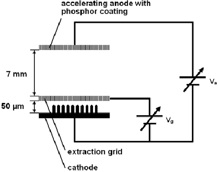
Figure 1. (a) Photograph of the FED device assembled in this study
(b) Schematic diagram of the FED device assembled in this study. Results and Discussion Figure 2 shows the SEM images of the Al:ZnO whiskers with a-CNx:H coating grown on the single crystalline silicon (100) wafer. The radius of curvature of the whisker tip was evaluated using the cross-sectional image. The top view (a) shows that the crystallites grew to sizes of about 0.7~1.0 mm with a density of 1×105 mm-2. The size of the crystallites was heterogeneous and the edge direction of each crystallite did not indicate any particular alignment. A cross-sectional SEM observation (b) reveals that the crystallites were whisker-shaped with an aspect ratio of 10. The deviation of the length of the whiskers was within 10~30%. The typical radius of curvature of the whisker tip was 85 nm. Although direct measurement of the resistivity of the Al:ZnO whisker is impossible, the Al:ZnO film exhibited a resistivity as low as 1 Ωcm, with an n-type characteristic. | 
| | Figure 2. SEM images of the Al:ZnO whiskers with a-CNx:H coating. | The fundamental field-emission property of the whisker emitter was examined under conditions of cathode-gate electrode distances of 50 µm and 300 µm. Figure 3 indicates gate electrode current (Ig) obtained at each distance. The threshold emission voltage Vth at 1 µA/cm2 for the distance of 50 µm was 120 V, corresponding to a value of 2.4 V/µm. It increased to 2.7 kV at 300 µm, that corresponds to a value of 9 V/µm. These threshold electric fields are higher than that (1.5~7.8 V/μm) reported previously [16]. This is explained as that the gate electrode captured only a part of current due to its mesh structure. 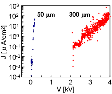
Figure 3. Cathode-gate electrode current obtained at each distance. Figure 4 shows the voltage and current profiles of the FED during operation. On the initial stage of the experiment, an accelerating voltage (Va) applied between the cathode and the anode was increased with an increment rate of approximately 12.5 V/s. In this procedure, phosphor showed no luminescence. As a next step, a gate voltage (Vg) applied between the cathode and the gate electrode was increased with an increment rate of approximately 4 V/s. When Vg reached to 800 V, Ig and anode current (Ia) increased suddenly followed by dropping Vg to 500 V. In this time, emitted electrons started to glow phosphor at the accelerating electrode. The Ia value was in the range of 0.3~1 mA. 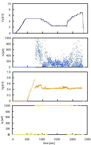
Figure 4. Voltage and current profiles of the FED during operation. | 


| | Figure 5. A series of photographs of red display device during operation. | Although Ig was saturated at 1 mA that is limit current of the Ig source, it dropped to zero when the Ia value increased to 1 mA. This induced the instability of the anode current or the phosphor glow intensity. After 900 s, Va was decreased slightly. The Ia value was also decreased to the range of 0.02~0.3 mA. After 1750 s, the Va value was increased to 7 kV again. The Ia value was also increased. The intensity of red phosphor was also changed with the variation of Va as indicated in Figure 5. A series of photographs of red display device shows that the intensity of the phosphor increased with the Va increment. Figure 6 shows the luminance of red display device as a function of Va. As evident from Figure 6 the luminance up to 88.9 cd/m2 can be achieved at 7 kV. | 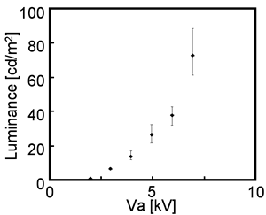
| | Figure 6. Luminance of red display device measured as the function of the anode voltage. | Summary The voltage and current profiles of the FED with the Al:ZnO cold emitter were measured during operation. Under conditions of Va of 5 kV and Vg of 500 V, the Ia value of 0.3~1 mA was obtained. This current range was enough to glow the ceramic phosphor for obtaining the intense luminescence. Acknowledgment This work was partially supported by a Grant-in Aid Scientific Research, the Ministry of Education, Culture, Sports, Science and Technology, contract No. 2267. The authors also thank to the support by the 21st century COE program at Nagaoka University of Technology. Reference 1. C. A. Spindt, I. Brodie, L. Humphrey and E. R. Westerberg, ”Physical properties of thin-film field emission cathodes with molybdenum cones”, J. Appl. Phys. 47 (1976) 5248-5263. 2. Y. Saito and S. Uemura, ”Field emission from carbon nanotubes and its application to electron sources”, Carbon 38 (2000) 169-182. 3. F. J. Himpsel, J. A. Knapp, J. A. VanVechten and D. E. Eastman, ”Quantum photoyield of diamond (111)—A stable negative-affinity emitter”, Phys. Rev. B 20 (1979) 624-627. 4. J. B. Cui, J. Ristein and L. Ley, ”Electron Affinity of the Bare and Hydrogen Covered Single Crystal Diamond (111) Surface”, Phys. Rev. Lett. 81 (1998) 429-432. 5. W. Mueller, H. S. Dewan, H. Chen, G. T. Mearini and I. L. Krainsky, ”Field emission from gated diamond arrays”,: Appl. Surf. Sci. 146 (1999) 328-333. 6. B. S. Satyanarayana, A. Hart, W. I. Milne and J. Robertson, ”Field emission from tetrahedral amorphous carbon”, Diam. Relat. Mater. 7 (1998) 656-659. 7. S. E. Huq, P. D. Prewett, J. C. She, S. Z. Deng and N. S. Xu, ”Field emission from amorphous diamond coated silicon tips”, Mater. Sci. Eng. B 74 (2000) 184-187. 8. M. Satoh, N. Tanaka, Y. Ueda, S. Ohshio and H. Saitoh, ”Epitaxial Growth of Zinc Oxide Whiskers by Chemical-Vapor Deposition under Atmospheric Pressure”, Jpn. J. Appl. Phys. 38 (1999) L586-L589. 9. H. Saitoh, M. Satoh, N. Tanaka. Y. Ueda and S. Ohshio, ”Homogeneous Growth of Zinc Oxide Whiskers”, Jpn. J.Appl. Phys. 38 (1999) 6873-6877. 10. H. Saitoh, Y. Namioka, H. Sugata and S. Ohshio, ”Nanoindentation Analysis of Al:ZnO Epitaxial Whiskers”, Jpn. J. Appl. Phys. 40 (2001) 6024-6028. 11. H. Saitoh, M. Satoh and S. Ohshio, ”Dendritic Side-Branching Observed on ZnO Epitaxial Whiskers”, J. Ceram. Soc. Jpn. 110 (2002) 693-695. 12. Y. Satoh, S. Oshio and H. Saitoh, ”Photoluminescence Properties of Y2O3: Eu Whiskers with Preferential <100> Orientation”, Jpn. J. Appl. Phys. 41 (2002) L1253-L1255. 13. H. Saitoh, Y. Okada and S. Ohshio, ”Synthesis of MgO/ZnO hetero-epitaxial whiskers using chemical vapor deposition operated under atmospheric pressure”, J. Mater. Sci. 37 (2002) 4597-4602. 13. H. Saitoh, N. Tanaka and S. Ohshio, ”Biaxial Rapid Epitaxy of Titanium Dioxide Crystals”, Chem. Vap. Deposition. 8 (2002) 267-272. 14. Y. Ohkawara, T. Naijo, T. Washio, S. Ohshio, H. Ito and H. Saitoh, ”Field Emission Property of Al:ZnO Whiskers Modified by Amorphous Carbon and Related Films”, Jpn. J. Appl. Phys. 40 (2001) 7013-7017. 15. H. Saitoh, H. Akasaka, T. Washio, Y. Ohkawara, S. Ohshio, H. Ito, ”Work Function of Amorphous Carbon Nitride with Various Functional Groups”, Jpn. J. Appl. Phys. 41 (2002) 6169-6173. 16. T. Inoue, S. Ohshio, H. Saitoh and K. Kamata, ”Preparation of nitrogen containing carbon films using chemical vapor deposition enhanced by electron cyclotron resonance plasma”, Appl. Phys. Lett. 67 (1995) 353-355. 17. D. Tanaka, S. Ohshio, J. Nishino and H. Saitoh, ”Indentation Creep of Nitrogen-Containing Carbon Films”, Jpn. J. Appl. Phys. 35 (1996) L1452-L1454. 18. H. Saitoh, T. Inoue and S. Ohshio, ”Solid Solubility of Nitrogen in Amorphous Carbon Films Deposited in Electron Cyclotron Resonance Plasma”, Jpn. J. Appl. Phys. 37 (1998) 4983-4988. 19. D. Tanaka, S. Ohshio and H. Saitoh, ”Time-Dependent Deformation Behavior of Amorphous Nitrogen-containing Carbon Films”, Jpn. J. Appl. Phys. 37 (1998) 6102-6106. 20. D. Tanaka, S. Ohshio and H. Saitoh, ”Nano-Indentation for Structural Analysis of Hydrogen- and Nitrogen-Containing Carbon Films”, Jpn. J. Appl. Phys. 39 (2000) 6008-6015. Contact Details | Hidetoshi Saitoh Department of Chemistry, Nagaoka University of Technology, Kamitomioka, Nagaoka, Niigata 940-2188, Japan E-mail: [email protected] | Tsukasa Washio Department of Chemistry, Nagaoka University of Technology, Kamitomioka, Nagaoka, Niigata 940-2188, Japan | | Shigeo Ohshio Department of Chemistry, Nagaoka University of Technology, Kamitomioka, Nagaoka, Niigata 940-2188, Japan | | |