Introduction The research on optical and electrical properties of CdS thin films has been of continuous interest due to their possible applications in the area of conversion of energy since such properties make them useful for building photovoltaic devices[1,2], sensors[3], among other applications. In this work we show that the CdS films can also be used for building analog multipliers or amplitude modulators. The principal purpose of every amplitude, frequency or phase modulator for analog or digital communication systems is to incorporate information to be transmitted (modulating signal) into a carrier signal. As a result of this process the Fourier spectrum of the modulating signal is shifted around the Fourier spectrum of the carrier signal generating side bands around it. As it is well known that the CdS is photoconductive [4,5], therefore to develop a device which takes advantage of such a property we characterized the photoconductivity, spectral response in the 590 to 451 nm range, and the conductivity at room temperature for polycrystalline CdS thin films doped with Erbium (CdS:Er). These films were grown by chemical bath deposition (CBD) with several levels of relative volume (R-V) of (Er(NO3)35H2O), where it was found that the process of doping inhibits the photoconductivity but improves the conductivity. Such decrement of the photoconductivity is explained by the measurement of the carrier density versus R-V at room temperature. After characterizing the CdS:Er samples we proceed to choose the most suitable sample to be used in conjunction with a conventional operational amplifier (OPAMP), with the purpose of building an amplitude modulator of double side band. Experimental The growth of CdS:Er was performed at 80 ± 1 °C on glass substrates. The details of the growth process have been previously reported[6]. Salt reagents (concentrations) used in the CdS:Er preparation were: CdCl2 (0.02 M), KOH (0.15 M), NH4NO3 (1.5 M), and SC(NH2)2 (0.2 M). The total solution (100 mL) for growing CdS was completed with relative volumes (R-V) of Er(NO3)35H2O in aqueous solution, with R-V ranging from 1.0 to 10.0 mL. This allowed the study of ten different doping levels. The sample labeled as Er0 corresponds to the undoped layer, and those labeled from Er1 to Er10 are ten increasingly doped samples. The photoconductivity was measured with a lock-in Standford Research Systems Model SR530 and a monochromator ScienceTech Inc. model 9490. The dark conductivity was measured with a programmable electrometer Keithley 617, and finally the carrier density was measured with a conventional apparatus from GMW Magnetic Systems model 3472-50. Two striped ohmic contacts separated 1cm were deposited on the CdS:Er samples in such a way that the area between the contacts was 1cm2 for all samples. With the Er8 sample an inverting amplifier (IA) was built by using a field effect transistor OPAMP TL081 as shown in Figure 1. In such a circuit, if the Ibias is negligible compared with the currents Ii and Isample, then the gain (GA) of the IA is simply , where Rsample is the resistance of the Er8 sample, and Ri is a resistance whose value is equal to Rsample. In order to make Ibias negligible Rsample must be much less 1/Ibias[7], for the TL081 Ibias≈50pA, and therefore the value of Rsample must be much less than 1011Ω. , where Rsample is the resistance of the Er8 sample, and Ri is a resistance whose value is equal to Rsample. In order to make Ibias negligible Rsample must be much less 1/Ibias[7], for the TL081 Ibias≈50pA, and therefore the value of Rsample must be much less than 1011Ω. 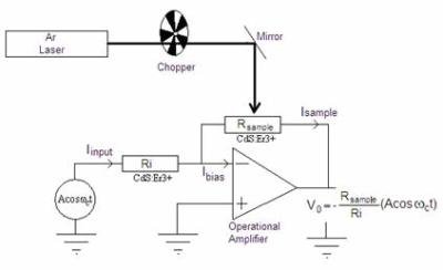
Figure 1. Experimental arrangement of the amplitude modulator for digital communications based on CdS:Er The IA was driven by a sinusoidal input (carrier signal) of five volts of amplitude at 5kHz of frequency, and the area of the sample was illuminated with a chopped Argon laser beam (multi line 488-514nm) with 2.2 mW of optical power. The chopped laser (200Hz of chopping frequency) represents a modulating signal of alternated cycles of illumination and darkness which could represent a digital signal of information to be transmitted; the experimental arrangement of the modulator is shown in the Figure 1. Finally the Fourier spectrum of the modulated signal obtained by the IA was measured with a Tektronix oscilloscope model TDS3012B. Results and Discussion We define the relative photoconductivity (δσ) of our samples of CdS:Er as 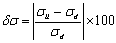 (1) (1)
where σd is the dark conductivity, and σil is the conductivity of the sample when it is being illuminated with white light. The Figure 2 is a graph of δσ versus R-V showing a decreasing trend of δσ as R-V is increased. 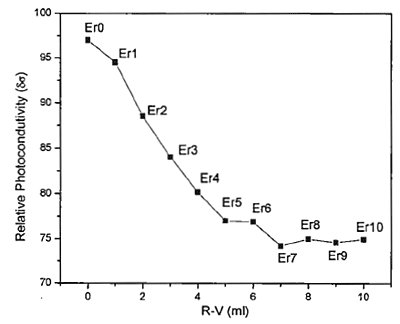
Figure 2. Photoconductivity δσ of the CdS:Er versus R-V For explaining this decrement we use the fact that the conductance (G) of the samples is directly proportional to its conductivity σ, G=kσ, where k is a proportionality constant which depends on the geometry of the sample, and using the following result [8] 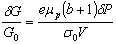 (2) (2)
where σ0 is the equilibrium conductivity, V is the volume of the sample, δP is the total excess number of holes produced by the incident radiation, μp is the mobility of the holes, b is the mobility ratio of the holes and electrons, and e is the magnitude of the electron charge. We can express the Eq. (2) in terms of the equilibrium carrier density of the electrons (n0) and holes (p0) through the definition of the conductivity 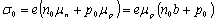 (3) (3)
Inserting Eq. (2) into Eq. (3), we finally obtain 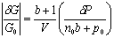 (4) (4)
In view of this expression the relative change of the conductance (δG/Go), and therefore the photoconductivity δσ, diminishes when the carrier density n0 or p0 is increased; in our case n0 was increased according to the studies of the carrier density by Hall effect (see Figure 3). 
Figure 3. Logarithm of the carrier density no of the CdS:Er versus R-V Figure 4 shows the conductivity σ versus R-V at room temperature, where an opposite behavior compared to δσ is observed, arising a conflict for photo-electronic applications because, as we mentioned before, the resistance of the sample must be much less than 1011Ω, but we also desire a large photoconductivity (δσ), and we choose the sample with higher conductivity, namely, the Er8 sample, forcing in this way to use higher optical power of light. 
Figure 4. Conductivity σ of the CdS:Er versus R-V The exit signal of the IA (V0) is the result of multiplying its input signal (Vi) by its gain GA, mathematically this can be expressed as  (5) (5)
In this manner, if Vi= Sinωct and if we modify the value of the resistance Rsample between two values, thus we could incorporate a binary signal of information into Vi. In order to achieve this goal we take advantage of the photoconductivity of the CdS:Er, specifically the fact that the conductivity (and consequently the resistance) changes when the sample Er8 is illuminated. In order to investigate the most suitable spectral range for illuminating the sample Er8 we measure the photocurrent of the sample Er8 as a function of the energy (wavelength) of the incident radiation; the outcome is shown in the Figure 5 where we realize that it is necessary to illuminate with energies greater than 2.4 eV, reason for which a HeNe laser whose wavelength is 633 nm can not be used for modifying the resistance of the CdS; instead, an argon laser operating at 488-514nm can successfully modify the resistance of the Er8 sample. 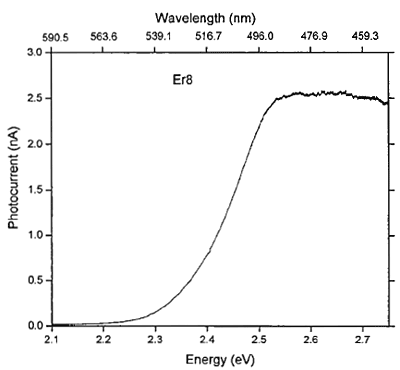
Figure 5. Spectral response of photocurrent of the Er8 sample At the top of the Figure 6 we present the exit signal V0 of the IA, where the carrier signal modulated in amplitude by the chopped laser can be observed. This signal could be feed to an antenna to travel to a remote place. At the bottom of the Figure 6 we show the Fast Fourier Transform (FFT) of V0, where the characteristic side bands corresponding to an amplitude modulated carrier signal are observed, demonstrating that we have successfully incorporated binary information into the carrier signal; the central peak corresponds to FFT of the carrier signal located at 5 kHz, the rest of the peaks are the double side bands spaced 200 Hz, each corresponding to the modulating signal. 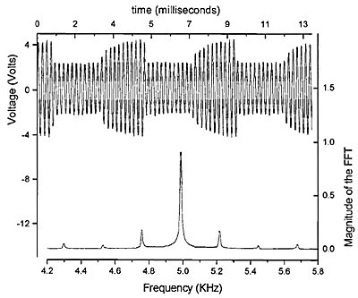
Figure 6. Output signal Vo and its Fast Fourier Transform Conclusions We have demonstrated that the CdS:Er can be used for developing optoelectronic systems for transmitting digital information which is the actual form of transmitting information, although our system is relatively slow (less than 1 kbit∕second) it has the advantage of being extremely simple compared with purely electronic modulators that use non linear devices like diodes, transistors, etc., and require electronic filters making them complex. The studies of the photocurrent versus the energy obtained in this work for CdS:Er show the spectrum range where it can be useful for optoelectronic purposes. References 1. C. S. Ferekides, D. Marinskiy, V. Viswanathan, B. Tetaly, V. Palekis, P. Selvaraj and D. L. Morel, “High Efficiency CSS CdTe Solar Cells”, Thin Solid Films, 361/362 (2000) 520-526. 2. J. Britt and C. Ferekides, “Thin film CdS/CdTe solar cell with 15.8% efficiency”, Appl. Phys. Lett. 62 (1993) 22. 3. B. K. Maremadi, K. Colbow and Y. Harima “A CdS photoconductivity gas sensor as an analytical tool for detection and analysis of hardous gases in the environment”, Rev Sci Instrum, 68 (1997) 3898-3903. 4. Toshio Yoshida, Takashi Oka and Michiharu Kitagawa, “Photoconductivity of CdS crystals irradiated with fast electrons”, Appl. Phys. Lett., 21 (1972)1. 5. Keiichi Yamamoto, Yoshimitsu Yamazoe, Shuichi Kameyama and Kenji Abe, “Measurement of the photoconductivity using the acoustoelectric of the surface wave ”, Appl. Phys. Lett., 29 (1976) 671. 6. J. L. Martínez, G. Martínez, G. Torres-Delgado, O. Guzmán del Ángel P, O. Zelaya-Ángel and R. Lozada-Morales, “Cubic CdS thin films studied by spectroscopic ellipsometry”, J. of Mater Sci. Mater Electron, 8 (1997) 399-403. 7. Sergio Franco, “Design with Operational Amplifiers and analog circuits”, McGraw-Hill, USA (1988) pp.194. 8. John P. Mckelvey “Solid State and Semiconductors Physics”, Robert E. Krieger Publishing Company, Inc., USA, (1982) pp. 353. Contact Details | J. A. Davila-Pintle
Facultad de Ciencias de la Electrónica
Benemérita Universidad Autónoma de Puebla
Puebla
México Email: [email protected] | O. Portillo-Moreno
Facultad de Ciencias Químicas
Benemérita Universidad Autónoma de Puebla
Puebla
México | | E. Molina Flores
Facultad de Ciencias de la Electrónica
Benemérita Universidad Autónoma de Puebla
Puebla
México | | |