Introduction Cadmium sulfide (CdS) films have been the subject of intensive research for its intermediate band gap, high absorption coefficient and reasonably efficient conversion to flat panel displays [1]. Also, they find applications in optoelectronic devices such as solar cells [2], nonlinear integrated optical devices and light emitting diodes (LEDs) or laser heterostructures for emission in the visible spectral range [3-4]. This material in thin film form has been grown by many deposition techniques [5-9], but Pulsed Laser Deposition (PLD) is known to be one of the best methods, because it preserves the stoichiometry under the right deposition conditions [10]. However, a major disadvantage of this technique is that the CdS target is difficult and poisonous to make and expensive to buy [11]. The problem of using commercial CdS-target is its high cost (50 mm Dia. x 3 mm, about 1350 Us dollars from Kurt J. Lesker). Although the use of the sinterized target is about twice as cheaper, its disadvantage is that the operator can have greater contact with the material during his manufacture. The major factor is that the cost of 3 gr of CdS pellets is about 30 times cheaper than the commercial CdS-target, therefore one of the main technological challenges for this process is to find a way that can offer lower cost, less contamination to the chamber and that the operator has the smaller contact with this material. In this work, we present the design, construction and the evaluation of a system for growth of CdS thin films using PLD. The suggested system Pulsed Laser Deposition Modified (PLD-M) in this work uses pellets as target in an ampoule with the capacity to control some of their properties, as a suitable process that fulfills the requirements mentioned above. Experimental The development of the PLD-M system (A schematic diagram of the general configuration is shown in Figure 1) consists: a stainless steel support (Figure 1(b)-A) placed inside the PLD chamber; a glass ampoule (6 mm in internal diameter and 93 mm in length, Figure 1(b)-C) that is held by two stainless steel holders (Figure 1(b)-B) attached to the support; a stainless steel cone (Figure 1(b)-E) that works like a chamber diaphragm that is placed over the ampoule and under the heating system (Figure 1(b)-F, G, H). Using the positioning holes (Figure 1(b)-I), the inclination angle of the ampoule can be changed. In its heating system, a dc power supply was used to drive current, I, through the nichrome wire (Figure 1(b)-H) having resistance R. Heating power, P, is generated simply by resistive heating: P=I2R. The critical requirements are that sufficient current be supplied to reach the desired substrate temperature. The heat generated is conducted through the carbon body (Figure 1(b)-H) by thermal conduction to the glass substrate (Figure 1(b)-G) on which the film is to be deposited. The thermometer is a thermocouple “K” bonded directly to the substrate (not showed). The substrate is mechanically attached placing it between the carbon body and cone to avoid outgassing of some organic solvents and binder from silver paint or paste by temperature. It was used a Nd:YAG laser (wavelength, pulse width and repetition rate of the laser are 355 nm, 15 ns and 10 Hz, respectively). The CdS pellets (from Alfa Aesar®, Ward Hill, MA, 99.999% purity, Figure 1(b)-D) were placed inside the ampoule that was exposed to a laser fluence of 2-4 J-cm-2 (Figure 1(b)-J), which causes a clearly visible plume luminescence in the ampoule body (Figure 1(b)-K). 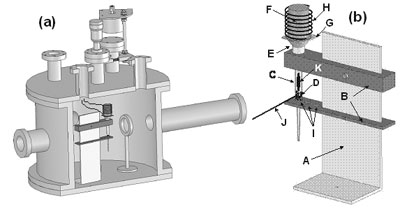
Figure 1. a) PLD-M Chamber and b) Block diagram of the ampoule system inside the PLD-M chamber: (A) Stainless steel support; (B) stainless steel holders; (C) glass ampoule; (D) CdS pellets; (E) stainless steel cone; (F) carbon heater body; (G) glass substrate; (H) Ni-Cr heating element; (I) positional holes; (J) laser beam and (K) plume plasma. Prior to film deposition, the glass substrates were thoroughly cleaned in a series of organic solvents by ultrasonic waves using acetone (CH3)2CO, methanol CH3OH and isopropanol CH3CHOHCH3, and then they were rinsed with deionized water and then dried with N2 gas. Also, the ampoule were thoroughly cleaned in a series of organic solvents by ultrasonic waves using: (CH3)2CO, CH3CHOHCH3 and xylene C6H4(CH3)2, and then they were rinsed with deionized water, then chemically cleaned in a HF and HNO3 solution (1:1 in volume) for approximately 10 min. After, the ampoule was heated to a temperature of about 300ºC for 12 h in an Ar atmosphere, the furnace was turned off and allowed to cool slowly to ambient temperature. Finally a small mass of pellets, 3 gr (20.7×10⁻³ moles), was placed in the ampoule and it was attached to system. The chamber was evacuated at 1x10⁻³ Pa, after that, it was flushed with Ar at 1x10⁻¹ Pa for 10 min. Finally, Ar was admitted in a controlled way to keep a working pressure of 1x10⁻¹ Pa. The deposit time was 2 minutes and the substrate temperature was kept at ~250ºC to within an accuracy of ±2ºC during the growth. Also, CdS films were grown by conventional PLD using a sintered CdS-target from powders processed by high energy ball milling, in order to compare their associated properties with those deposited by PLD-M under same the procedure and deposition conditions. After the deposition, the thickness of the deposited films was measured using a Dektak3ST profilometer by Veeco Instruments. The chemical compositions of samples were measured with an Electron Dispersive Spectroscopy (EDS) detector attached to a scanning Electron Microscope (SEM) (JSM-5300, Jeol). The surface morphology of the films was assessed by an atomic force microscope (AFM) using tapping mode. The X-ray diffraction (XRD) measurement was performed with a Siemens D5000 using the CuKα line (λkα1 = 1.54056 Å and λkα2 = 1.54439 Å) with Bragg Brentano measurement geometry (The resolution in angle of the diffractometer was 0.050°). Optical transmittance spectra of the films were recorded on a Perklim Elmer Lamda UV-VIS spectrophotometer. Raman spectra were taken using the 488 nm line of an argon laser as the light source in the backscattering geometry at room temperature. A Raman spectrometer built around a double grating monochromaton SPEX model 14018 was used. Results and Discussion During film deposition in PLD-M, the process deposition shows the formation of three zones inside the ampoule, Figure 2, which is not fully understood. The geometry and expansion direction of the plume in PLD-M depend on ampoule arrangement. Because material ablation is made inside the ampoule, only a small quantity of material is necessary and also that the vapor density rises and collisions occur in the ampoule surface avoiding that the evaporated material reaches the chamber wall proving less contamination and a cleaner system to the operator in comparison with the target. 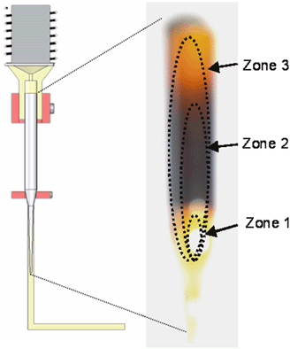
Figure 2. The formation of the three zones during process deposition. The structural study of the CdS films performed by XRD measurements (scanning 2θ in the range 20-60°) is shown in Figure 3. The film CdS is hexagonal (ICSD, Inorganically Crystal Structure Database, card 60629 and PDF, Power Diffraction File, card 751545) as seen from the typical diffraction peaks from planes such as (100), (002), (101), (102), (110), (103), (200) and (112). In order to determine the position of the peaks, they were adjusted to a Pseudo-voight function which is a combination of the functions Gaussian (G) and Lorenzian (L) of the form: ηL + (1-η)G, where η is the parameter of the mixed function. The parameters of lattice of the unitary cell (a0 = 4.14 Å and c0 = 6.71 Å) were obtained for refinement using the Celref program [12]. A comparison of the XRD spectra with that of PLD-M reveals a better structural quality in films deposited by pellets. 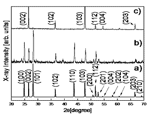
Figure 3. XRD patterns of CdS films deposited under two different conditions. a) Reference pattern of hexagonal CdS, b) pattern CdS film for PLD-M and c) pattern CdS film for PLD conventional. The AFM micrographs indicate a grain size of 0.1µm, as shown in Figure 4. The films CdS were: of color transparent yellow, uniform thickness, and strongly stick to the surface of the substrate, and the roughness is less than 2 Ǻ (rms). The grains of CdS films grown by conventional PLD (Figure 4-a) are deformed in random direction and there are roughness presented on each grain, while grains of films grown by PLD-M (Figure 4-b) have similar size and slightly less rough surface. This can be due to the greater kinetic energy distributed by the angular distribution of the plume plasma and the flux of species [13-17]. Optical band gap of CdS film can be determined from the sharply falling transmission region. According to Tauc's law, the absorption coefficient has the following energy dependence: α = B(hv-Eg)2/hv [21]. So the straight line plot between (αhe)1/2 (α is the absorption coefficient) vs. photon energy (hv) in the wavelength range 450-750 nm, would provide the value of the optical band gap (Eg). Even though the films deposited by PLD and PLD-M were grown at the same conditions, the Figure 6 shows the band gap energy of the CdS films grown by PLD-M was found to be 2.56 eV where this higher value of Eg on films could be associated to the crystallite size or the short deposition time. In this sense, the AFM data are consistent indicating the presence of smaller crystallites in the films. 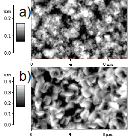
Figure 4. An AFM image of the CdS films prepared by: a) (1x 1μm2) PLD conventional and b) (1x 1μm2) PLD-M. 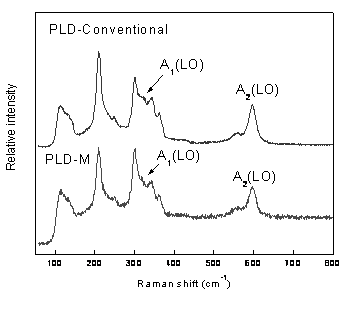
Figure 5. Raman spectra of CdS films, deposited for PLD-conventional and PLD-M. 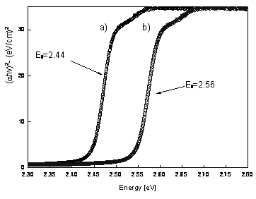
Figure 6. Plots of (αhv)2 versus photon energy (hv) of the CdS films, showing an optical bandgap. a) 2.44 eV for CdS films grown for PLD and b) 2.56 eV for CdS films grown for PLD-M. Conclusions Figure 5 shows the comparison in wavenumber of longitudinal-optical LO modes of films grown by conventional PLD with those of films CdS by PLD-M. A Lorentzian line shape is fitted to the Raman spectra to find the peak position and full width at half maximum (FMHM). Two peaks are observed at around 302 cm-1 and 596 cm-1, respectively. The Raman peak at 302 cm-1 is attributed to A1(LO) phonon in CdS [18] and the peak at 596 cm-1 is attributed to the A2(LO) phonon [19]. The FMHM of the peak is 19 cm-1 that is much larger than a CdS single crystal one (6.5 cm-1) and although that this usually indicates poor crystallinity in films, the well defined peaks observed from the XRD pattern indicate the good crystalline nature of the films, hence this higher FWHM in the present case can be attributed to the polycrystalline effect in the deposited film [20]. The results obtained above suggest that this design PLD-M, is not only a suitable way to be used for the growth of films of CdS, also it improves a lower cost, minor contamination technique to the chamber and operator and the using of commercial materials in its manufacture. The films obtained by this design are homogeneous and uniform without holes. Acknowledgements This work was supported by grants of CGPI-IPN, Proj. No. 20060505. Thanks are due to F. Chale Lara and J. Zapata Torres for their technical help. References 1. F. El-Akkad, and M. A. Naby, “Properties of RF-sputtered CdS Thin Films”, Solar Energy Materials, 18, 151-158 (1989). 2. S. Chandra, R. K. Pandley and R. C. Agrawal, “Solar Energy Conversion by Photoelectrochemical Cells using Chemical-bath-deposited CdS Films”, J. Phys. D: Appl. Phys., 13, 1757-1760 (1980). 3. C. M. Dai, L. Horng, W. F. Hsieh and Y. T. Shih, “High Orientation CdS Thin Films Grown by Pulsed Laser and Thermal Evaporation”, J. Vac. Sci. Technol. A, 10, 484 (1992). 4. J. Alex Chediak, Z. Luo, J. Seo, N. Cheung, L. P. Lee and T. D. Sands, “Heterogeneous Integration of CdS Filters with GaN LEDs for Fluorescence Detection Microsystems,” Sensors Actuators A, 111, 1 (2004). 5. B. Ullrich and R. Schroeder, “Green Single- and Two-photon GAP Emission of Thin-film CdS Formedby Infrared Pulsed-laser Deposition on Glass“, IEEE J. Quantum Electron, 37, 1363-1367 (2001). 6. H. Wang, Y. Zhu and P. Ong, “Rotary Target Method to Prepare Thin Films of CdS/SiO[2] by Pulsed Laser Deposition”, J. Cryst. Growth, 220, 554 (2000). 7. T. Hayashi, T. Nishikura, T. Susuki and Y. Emma, “Formation and Properties of In-doped High-conductivity CdS Film”, J. Appl. Phys., 64, 3542-3550 (1988). 8. I. Kaur, D. K. Pandya and K. L. Chopra, "Growth Kinetics and Polymorphism of Chemically Deposited CdS Films", J. Electrochem. Soc., 127, 943 (1980). 9. M. Khanlary, P. Townsenda, B. Ullrich and D. E. Hole, “Ion-beam Luminescence of Thin-film CdS on Glass Formed by Pulsed-laser Deposition” J. Appl. Phys., 97 (2005) 023512.1-023512.4 10. J. T. Cheung and H. Sankur, “Growth of Thin Films by Laser-induced Evaporation”, CRC Crit. Rev. Solid State Mater. Sci., 15, 63 (1988). 11. D. B. Chrisey and G. K. Hubler, “Pulsed Laser Deposition of Thin Films”, Wiley Interscience, New York, (1994) pp. 87-90. 12. J. Laugier and B. Bochu, “CELREF Unit-Cell Refinement Software on a Multiphase System”, Laboratoire des Matériaux et du Génie Physique Ecole Nationale Supérieure de Physique de Grenoble (INPG). 13. A. V. Bulgakov and N. M. Bulgakova, “Gas-dynamic Effects of the Interaction between a Pulsed Laser-ablation Plume and the Ambient Gas: Analogy with an under Expanded Jet”, J. Phys D: Appl. Phys., 31, 693-703 (1998). 14. R. Kelly, “Gas Dynamics of the Pulsed Emission of a Perfect Gas with Applications to Laser Sputtering and to Nozzle Expansion”, Phys. Rev. A, 46, 860-874 (1992). 15. A. V. Bulgakova and N. M. Bulgakova, ”Dynamics of Laser-induced Plume Expansion into an Ambient Gas during Film Deposition”, J. Phys. D: Appl. Phys., 28, 1710 (1995). 16. M. Aden, E. W. Kreutz and A. Voss, “Laser-induced Plasma Formation during Pulsed Laser Deposition“, J. Phys. D: Appl. Phys., 26, 1545-1553 (1993). 17. K. R. Chen, J. N. Leboeuf, R. F. Wood, D. B. Geohegan, J. M. Donato, C. L. Liu and A. A. Puretzky, “Laser-solid Interaction and Dynamics of Laser-ablated Materials”, Appl. Surf. Sci., 96 (1996) 45. 18. B. Tell , T. C. Damen and S. P. S. Porto, “Raman Effect in Cadmium Sulfide”, Phys. Rev., 144, 771-774 (1966). 19. M. Ichimura, A. Usami, T. Wada, M. Funato, K. Ichino, S. Z. Fujita and S. G. Fujita, “Raman Spectra of Cubic Zn1-xCdxS”, Phys. Rev., 46, 4273-4276 (1992). 20. M. Froment, M. C. Bernard, R. Cortes, B. Mokili and D. Lincot, “Study of CdS Epitaxial Films Chemically Deposited from Aqueous Solutions on InP Single Crystals”, J. Electrochem. Soc., 142, 2642-2649 (1995). 21. J. I. Pankove, “Optical Processes in Semiconductors”, (Ed. Dover), New York, (1971) pp. 44-87. Contact Details |