Bruker has introduced an advanced FT-IR spectroscopic system, called nanoIR3-s, that combines scattering scanning near-field optical microscopy (s-SNOM) and nanoscale IR spectroscopy (AFM-IR) with an in-built atomic force microscope (AFM), all incorporated into a single system.
Built on the legacy of Anasys technology’s know-how in AFM-based nano-optical characterization, the nanoIR3-s system provides optical property mapping, nanoscale IR spectroscopy, and chemical imaging with 10-nm spatial resolution, as found on 2D material samples.
The nanoIR3-s system also enables AFM material property mapping and AFM topographic imaging, with nanometer-scale resolution. Capabilities like these make nanoIR3-s the preferred instrument for correlative analyses across numerous applications in material science.
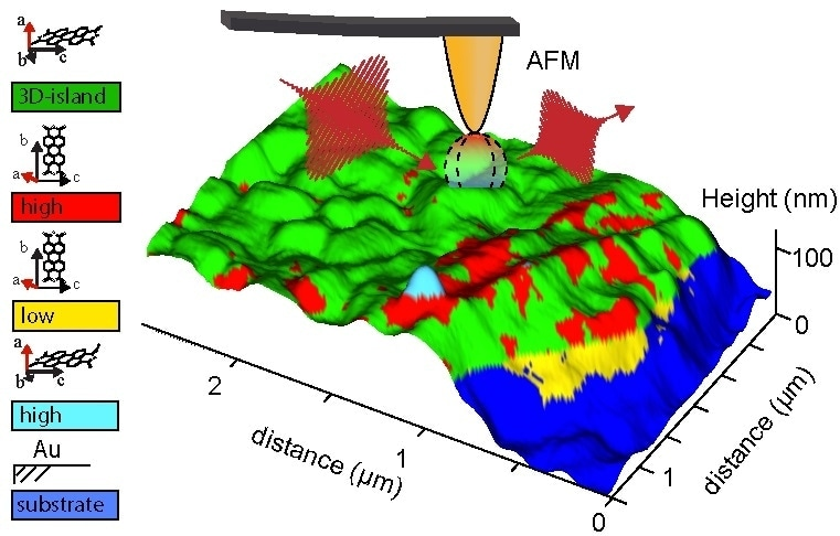
Correlative analysis of spatial map reconstructed from separate correlated AFM and chemical measurements reveal the molecular orientation of vacuum-deposited PTCDA defects. Image Credit: Science Advances 2 (10), e1601006 - E. A. Muller, et al.
Features
- Femtosecond broadband nano-FTIR spectroscopy
- Complementary s-SNOM and AFM-IR methods
- Fully featured, high-resolution AFM with electrical, mechanical, and thermal modes
Complementary Nanoscale Techniques
s-SNOM
Both the near-field phase and amplitude of the dispersed light are established with the help of patented techniques meant for s-SNOM. This can be realized as the probe scans across the sample surface to create near-field optical images that correspond with the topography image.
The probe can also be positioned at a fixed site and the wavelength of the source can be modified to offer near-field spectra. POINTspectra is a patented capability that provides both chemical imaging and spectroscopy for CW QCL laser operation.
Tapping AFM-IR
Tapping AFM-IR employs the same photothermal detection mechanism as that of resonance-enhanced AFM-IR, but the Tapping AFM mode operation is applied as the sensing mechanism. A uniquely developed Tapping AFM-IR probe is also driven at different harmonic modes/resonances to spot photothermal expansion.
Using the Tapping AFM-IR, the sample is subjected to lower AFM probe forces to obtain higher spatial resolution chemical imaging to 10 nm or less, based on the sample type.
Resonance-Enhanced AFM-IR
The resonance-enhanced AFM-IR component within the instrument operates by lighting up the sample in a top-down manner with a broadband, tunable, pulsed mid-IR laser. The pulsed radiation is selectively absorbed by the sample. This leads to a rapid and fleeting local expansion, which is identified by the resulting mechanical deflection of the AFM probe.
The resulting IR absorbance spectra can be directly linked to the FT-IR absorbance spectra, allowing seamless interpretation. These IR absorbance spectra can be investigated against the available IR spectral database libraries.
Mechanical Property Mapping, NanoThermal Analysis, and Electrical AFM Modes
In addition to nanoscale IR spectroscopy, the nanoIR3-s system can quantify contact resonance frequencies of an AFM cantilever through the Lorentz Contact Resonance (LCR) method. This feature allows users to map the variations in the mechanical properties of a sample.
The nanoTA method can also be used for imaging local thermal properties to perform quantitative measurements of thermal transition temperatures at nanoscale spatial resolution.
 Download: Chemical Characterization of Polymeric Films, Blends, and Self-Assembled Monomers
Source: Bruker Nano Surfaces
| Modes |
| Chemical Imaging Modes |
Tapping AFM-IR; FASTspectra (AFM-IR); FASTmapping (AFM-IR); Hyperspectral Imaging; s-SNOM |
| AFM Modes |
Standard: tapping; contact phase; force calibration; lateral force; EFM/MFM Optional: NanoTA; SThM; LCR; C-AFM; KPFM |
| Key Laser Options |
| POINTspectra QCL Laser |
6 or 4 chip continuous wave/pulsed with 950-1900 cm-1 range for s-SNOM and AFM-IR, additional wavelengths available upon request |
Single/Multiple Chip QCL
Laser |
Single or multi-chip continuous wave/pulsed with different spectral ranges for s-SNOM |
| CO2 Laser |
For use with s-SNOM |
Visible 632.8 nm
HeNe Laser |
10 mw and optics package for integration into nanoIR3-s |
| 1550 nm NIR Diode Laser |
5 mw and optics package for integration into nanoIR3-s |
| AFM Performance |
| Z Noise |
<100 pm RMS |
| XY Scan Range |
50 µm x 50 µm |
| Z Range |
>4 µm |
| Scan Resolution |
≤1024 x 1024 pixels |
| XY Scan Stage |
Flexure with capacitive closed-loop sensing |
| Tip Positioning Accuracy |
±10 nm |
| Sample Size and Movement |
| Sample Size |
<25 mm dia max |
| Sample height |
<10 mm max |
| XY Stage Range |
8 x 8 mm motorized |
| Z stage Range |
>5 mm motorized |
| Optical Microscopes |
| Illumination |
Brightfield |
| CCD Resolution |
1.5 µm 5 MP |
| Digital Zoom |
3X |
| Objective |
10X |
| Field of view |
~900 x 600 µm max; ~450 x 300 µm min |
Download the full datasheet for the Anasys nanoIR3-s.