The Lawrence Berkeley National Laboratory has developed the Semiconductor High-NA Actinic Reticle Review Project (SHARP) microscope for photolithography. The SHARP microscope is an advanced extreme-ultraviolet (EUV) photomask-imaging microscope, which has been developed in partnership with semiconductor manufacturers.
Kenneth Goldberg at the Berkeley Lab's Materials Science Division Center for X-Ray Optics (CXRO) is leading the 1.5-year, $4.1 million project. The EUV microscope is to be used simultaneously along with the Advanced Light Source microscope at beamline 11.3.2. The Actinic Inspection Tool (AIT) microscope has specific imaging capabilities, but may not be able to meet future requirements. SHARP will be better than the AIT in terms of speed, resolution, coherence control and illumination.
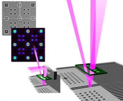 At top left are programmed pattern defects, including the large protrusion in the center, developed by a team at IBM to evaluate printing sensitivity. The current AIT microscope's image of the defects is center left. The final stage of the AIT's beam path is shown bottom left: the synchrotron's EUV beam enters from the top, reflects from the mask, is focused by an array of zone plates, and then reflects from a turning mirror to an EUV-sensitive camera, not shown, to the left. The more efficient SHARP beam path at right removes the turning mirror and a window from the array of zone plates to increase brightness. SHARP incorporates other refinements such as a new high-efficiency illuminator, a tunable monochromator that controls the coherence of the light, and a choice of zone plate lenses for different magnifications as the microscope navigates around the mask. Credit: Lawrence Berkeley National Laboratory
Semiconductor devices of the near future will measure in terms of billionths of a meter – 8, 11 or 16 nm. Mass production of such semiconductors requires a 13.5 nm wavelength EUV light for photolithography. Photomasks play a major role in mass production in lithography. Master circuit patterns are carried by a series of photomasks and are transferred layer by layer onto chips for creation of semiconductor devices.
Dust particles or imperfections on the master circuit patterns can lead to chip failure. EUV microscopy can reliably identify such particles and defects when compared to non-EUV inspection tools. It can help evaluate defects and repair mask architectures and materials, advanced pattern features and strategies.
The SHARP EUV microscope has high-magnification objective lenses, which are holographic Fresnel zoneplate lenses. CXRO's Nanowriter produces these lenses, which have a width slightly more than a single human hair. These microscopic lenses can project images with a 2,000x magnification. Illumination coherence control is a unique feature of the microscope. The EUV beam produced has a laser-like coherence. Re-engineering the illumination into a partial coherence state can improve the image resolution for microscopy. The beamline illuminator in the SHARP microscope has an angle-scanning mirror that can maneuver the highly-coherent ALS light into patterns and break and re-shape the coherence properties.