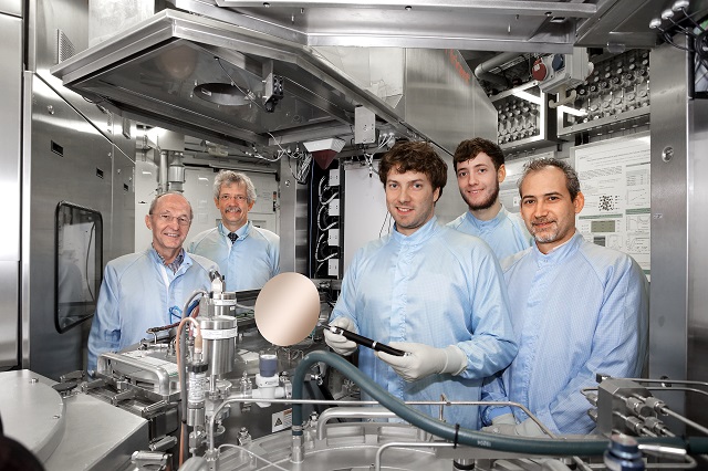
 Scientists from the Peter Grünberg Institute (PGI-9) standing next to a CVD system which was used to prepare and develop parts of the new laser (from left: Prof. Siegrfried Mantl, Prof. Detlev Grützmacher, Stephan Wirths, Nils von den Driesch, and Dr. Dan Mihai Buca. Copyright: Forschungszentrum Jülich
Scientists from the Forschungszentrum Jülich and the Paul Scherrer Institute in Switzerland have collaborated with global partners to build a germanium-tin (GeSn) semiconductor laser for applications in silicon chips.
This semiconductor is made up only of main group IV elements, and hence the GeSn laser can be applied onto silicon chips directly. A new method for data transmission using light on computer chips is offered by this semiconductor. The speed of data transfer is faster and requires only a fraction of the energy that is required when compared to data transmission through copper wires.
In present day computer technology, the data transfer that takes place between multiple cores and also between memory cells and logic elements is considered to be a bottleneck. Data transmission using light could help address this bottleneck, and could offer more energy efficient and faster data flow between various board components, and also on computer chips. "Signal transmission via copper wires limits the development of larger and faster computers due to the thermal load and the limited bandwidth of copper wires. The clock signal alone synchronizing the circuits uses up to 30% of the energy – energy which can be saved through optical transmission," explains Prof. Detlev Grützmacher, Director at Jülich's Peter Grünberg Institute.
Optical connections have been used by computing centres and long-distance telecommunication networks for a very long period. Even over long distances these optical connections permit very high bandwidths. The signal propagation through optical fibers is possible simultaneously across different wavelengths and there is hardly any loss. The speed achieved benefits nano- and micro electronics. "The integration of optical components is already well advanced in many areas. However, in spite of intensive research, a laser source that is compatible with the manufacturing of chips is not yet achievable," according to the head of Semiconductor Nanoelectronics (PGI-9).
Silicon belongs to the main group IV elements of the periodic table. This material forms the basis for chip manufacturing. Semiconductor lasers made from gallium arsenide are used for telecommunication systems. These lasers are made up of the main group III or V elements, and are expensive. This affects crystal properties and hence such components of the laser cannot be applied onto silicon directly. Other methods have to be used. They can be manufactured externally, however they require great effort. The components then have to be glued to the silicon wafer. A major disadvantage is that the thermal expansion coefficients of these elements and that of silicon are different. This reduces the lifetime of these types of components.

Scientists from the Peter Grünberg Institute (PGI-9) standing next to a CVD system which was used to prepare and develop parts of the new laser (from left: Prof. Siegrfried Mantl, Prof. Detlev Grützmacher, Stephan Wirths, Nils von den Driesch, and Dr. Dan Mihai Buca. Copyright: Forschungszentrum Jülich
Semiconductors made of main group IV elements can be easily integrated into processes for production. However, germanium and silicon elements of main group IV are not very efficient light sources, and they are classified as indirect semiconductors. When compared to direct semiconductors, they emit very little light and mostly as heat when excited. This has made researchers worldwide to conduct studies on germanium to make it a laser source by amplifying optical signals.
Researchers at Jülich's Peter Grünberg Institute have combined germanium and tin to successfully create a "real" direct main group IV semiconductor laser.
"The high tin content is decisive for the optical properties. For the first time, we were able to introduce more than 10% tin into the crystal lattice without it losing its optical quality.
PhD student Stephan Wirths
The functioning of the laser is so far limited to low temperatures of up to minus 183 degrees Celsius, however. This is mainly due to the fact that we worked with a test system that was not further optimized.
Dr. Dan Buca
Wirths collaborated with Prof. Siegfried Mantl's group at PGI-9 to apply the laser onto a silicon wafer directly. Researchers then measured the properties of the material were then measured at the Paul Scherrer Institute. The laser structures were fabricated by Richard Geiger, a PhD student, at the Institute. "That way, we were able to demonstrate that the germanium-tin compound can amplify optical signals, as well as generate laser light," reports Dr. Hans Sigg from the Laboratory for Micro and Nanotechnology.
For the demonstration, the researchers excited the laser optically. Scientists belonging to Dr. Dan Buca's group at Jülich are trying to link the electronics and optics more closely. Further progress would involve use of electricity for generating laser light, possibly without cooling. The researchers plan to make an electrically pumped laser that has the ability to function at room temperature.
The laser beam that is generated is invisible and cannot be seen with the naked eye. GeSn absorbs light and then emits them in about 3µm wavelength range. This is the boundary between mid- and near wavelength infrared. Greenhouse gases, biomolecules, and other such carbon compounds demonstrate strong absorption lines at this boundary. Therefore sensors made using GeSn offer a new way to detect these compounds.
The new laser material may benefit new applications that may possibly be expensive. They may also benefit computer chips. For medical applications, implantable chips or gas sensors could be used for acquiring blood sugar levels and other such information. Further development could lead to portable, inexpensive sensor technology that could provide real-time data for weather and climate applications. This sensor technology could possibly be integrated into smart phones.
The results of this study have been published in Nature Photonics journal.
References