Jan 12 2018
A new synthesis process for low-cost fabrication of a material for infrared cameras has been developed by scientists at the U.S. Army Research Laboratory and Stony Brook University. This new development makes room for new possibilities for future Army night-time operations.
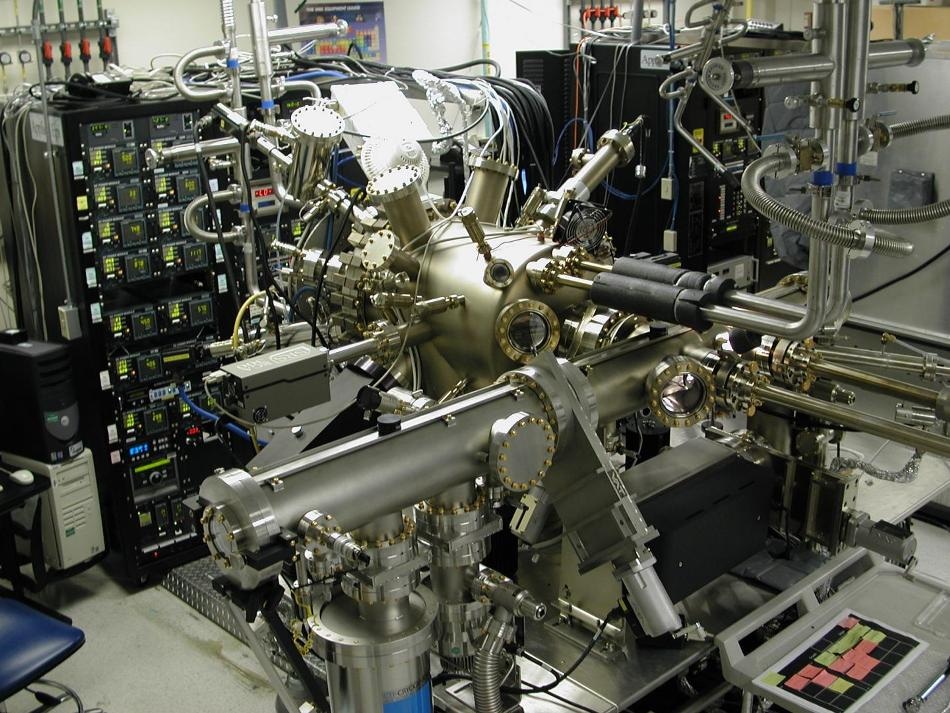 The Molecular Beam Epitaxy (MBE) is being used by Army researchers to produce new infrared detector materials based on InAsSb. This is a III-V semiconductor, a class of materials also used in opto-electronics in many commercial products such as DVD players and cell phones. (Photo credit: US Army)
ARL's Drs. Wendy Sarney and Stefan Svensson headed an exceptional approach for employing the semiconductor InAsSb, a material that has not been earlier used in high-performance IR cameras for the longest wavelengths (10 μm). The best materials for the IR camera light-sensors are presently based on HgCdTe, which is from the family of II-VI compounds.
"Unfortunately, they are very expensive, mostly because there are only military customers for this material," Svensson said.
InAsSb is a III-V semiconductor, which is a class of materials employed in opto-electronics in a number of commercial products such as cell phones and DVD players.
"The human eye is optimized by nature to observe reflected light from the sun in a very narrow band of colors (wavelengths of light), known as the visible spectrum; however, all objects in nature glow with a faint light even at low temperatures, which produces colors in the infrared (IR) range which are invisible to the naked eye. These wavelengths are about ten times longer than those of visible light.
"By using cameras that can see the faint IR light, soldiers can operate during night times," Sarney said. "The more sensitive such a camera is, or in other words, the smaller the color or temperature differences are that it can see, the more details that can be discerned on a battlefield and enemies can be detected at longer ranges. High-performance IR cameras are therefore extremely important for the Army."
The key in this discovery refers to the realization that the material had to be undistorted by strain to see at 10 μm. This was a key difficulty that had to be overcome before InAsSb could be employed as a sensor material. The performance of devices based on semiconductor materials also relies on the crystalline perfection of the material. It is necessary for InAsSb to be deposited onto a starting crystalline material (a substrate) which comprises of a smaller spacing between the atoms. This mismatch in size at the atomic scale must be managed very well in order to allow proper working of the light-sensitive material.
Among possible substrates, cheaper and larger ones usually have progressively smaller atomic spacing. Over several years Stony Brook and ARL discovered a way for managing the atomic spacing mismatch culminating in the present work, which employs GaAs as a substrate. This is considered to be the most common substrate employed in the III-V industry for a number of consumer products. It is available in large sizes and is inexpensive. Large area substrates permit manufacturing of multiple camera sensors simultaneously, which could be performed in commercial foundries. All this makes way for new opportunities to develop high-quality IR cameras ideal for soldiers in a much economical manner.
Stony Brook and ARL combined strain-mediating techniques to efficiently manage the 10% atomic spacing mismatch between the GaAs substrate and InAsSb sensing material. To perform this, an intermediate layer of GaSb was deposited on GaAs in a manner that trapped most of the defects brought about by the mismatch in size. They then went on to increase the atomic spacing with a graded layer that also prevented defects from the InAsSb sensor material.
High resolution transmission electron microscopy was used for examining the material in order to ensure that it had adequate structural quality. They also discovered that the optical quality related to detection properties was extraordinarily high. This research demonstrates a path to a lower cost, practical solution for the eventual fielding of night-vision systems based on III-V long wavelength infrared materials.